STM32 Architecture: Difference between revisions
No edit summary |
|||
| (139 intermediate revisions by the same user not shown) | |||
| Line 1: | Line 1: | ||
=Introduction= | =Introduction= | ||
My knowledge is very small, no not just in general, but on this subject in computers. This is probably where I regret not having a degree. But here goes I am going to try and understand enough of the diagram from the STM32F0xx Cortex-M0 to be dangerous. | My knowledge is very small, no not just in general, but on this subject in computers. This is probably where I regret not having a degree. But here goes I am going to try and understand enough of the diagram from the STM32F0xx Cortex-M0 to be dangerous. | ||
[[File:STM32F0xx Cortex-M0 System Overview.png| 400px]]<br> | [[File:STM32F0xx Cortex-M0 System Overview.png| 400px]]<br> | ||
I am again looking at Intermation and their course which is Computer Organization and design. | I am again looking at Intermation and their course which is Computer Organization and design. | ||
=NVIC and EXTI= | |||
Not fully on board with this but the NVIC (Nested Vectored Interrupt Controller) is a interrupt controller connected to the CPU. From one of the docs (STM32G4) it lists its features as | Not fully on board with this but the NVIC (Nested Vectored Interrupt Controller) is a interrupt controller connected to the CPU. From one of the docs (STM32G4) it lists its features as | ||
*102 interrupt sources, | *102 interrupt sources, | ||
| Line 118: | Line 12: | ||
In the lesson I was doing this came up because of the EXTI (EXTernal Interrupt/Event) controller which is connected to the NVIC. When using CubeMX you can configure handlers for the GPIO pin which connects to the EXTI on the NVIC. In my case there are 28 lines on the EXTI<br> | In the lesson I was doing this came up because of the EXTI (EXTernal Interrupt/Event) controller which is connected to the NVIC. When using CubeMX you can configure handlers for the GPIO pin which connects to the EXTI on the NVIC. In my case there are 28 lines on the EXTI<br> | ||
[[File:NVIC EXTI.png|400px]] | [[File:NVIC EXTI.png|400px]] | ||
=Pending Request Register= | |||
When we press a button it is flagged in the pending request register shown above. We can get the address of the register from the manual. In the case of the STM32F302R8 we can first find the EXTI in the manual<br> | When we press a button it is flagged in the pending request register shown above. We can get the address of the register from the manual. In the case of the STM32F302R8 we can first find the EXTI in the manual<br> | ||
[[File:STM32F302R8 EXTI.png|400px]]<br> | [[File:STM32F302R8 EXTI.png|400px]]<br> | ||
| Line 126: | Line 20: | ||
They were very keen to stress that it is the programmers (so old fashioned) job to clear the bit in the PR when done. Using the CubeMX this is what is generated for you via macros.<br> | They were very keen to stress that it is the programmers (so old fashioned) job to clear the bit in the PR when done. Using the CubeMX this is what is generated for you via macros.<br> | ||
[[File:STM32 EXTI Handler.png|400px]]<br> | [[File:STM32 EXTI Handler.png|400px]]<br> | ||
=STM32 Header Files= | |||
Briefly ARM have a thing called CMIS. Vendors follow these guidelines and share common macros etc. | Briefly ARM have a thing called CMIS. Vendors follow these guidelines and share common macros etc. | ||
==Volatile Keyword== | ==Volatile Keyword== | ||
| Line 155: | Line 49: | ||
} | } | ||
</syntaxhighlight> | </syntaxhighlight> | ||
=GPIO and Ports= | |||
==Resetting Ports== | |||
Again for documentation most of the STM32 boards will list the peripheral and have the register as the last entry. When you look at the ports some of the reset value might not be neccessarily 0x000 0000. For the STM32F302R8 they were<br> | Again for documentation most of the STM32 boards will list the peripheral and have the register as the last entry. When you look at the ports some of the reset value might not be neccessarily 0x000 0000. For the STM32F302R8 they were<br> | ||
'''Address offset:0x00'''<br> | '''Address offset:0x00'''<br> | ||
| Line 163: | Line 57: | ||
*Reset value: 0x0000 0000 for other ports | *Reset value: 0x0000 0000 for other ports | ||
Each GPIO should have a pullup resistor. This ensures pins are not floating,neither positive or negative, which will happen due to residual voltage. The pullup resistor value can be found in the documentation searching for Rₚᵤ. or Weak Pull-up.<br> | Each GPIO should have a pullup resistor. This ensures pins are not floating,neither positive or negative, which will happen due to residual voltage. The pullup resistor value can be found in the documentation searching for Rₚᵤ. or Weak Pull-up.<br> | ||
==GPIO Modes== | |||
A bit was said about this and the importance of using pullup resistors. The open drain setting was brought up with I2C so may come back to this. | A bit was said about this and the importance of using pullup resistors. The open drain setting was brought up with I2C so may come back to this. | ||
*Input | *Input | ||
| Line 169: | Line 63: | ||
**Push/Pull (0 or 1) | **Push/Pull (0 or 1) | ||
**Open Drain (0 or floating) | **Open Drain (0 or floating) | ||
== | ==Speed (Output Only)== | ||
We can set the speed of the output using the OSPEEDRy. There are two bits for each port this effect the rising time and falling time. You have to refer to the datasheet (separate from reference manual) to understand the different available speeds. Search for OSPEEDS. I will be very happy if I ever need this. The speed are based on the voltage and clock capacitance.<br> | We can set the speed of the output using the OSPEEDRy. There are two bits for each port this effect the rising time and falling time. You have to refer to the datasheet (separate from reference manual) to understand the different available speeds. Search for OSPEEDS. I will be very happy if I ever need this. The speed are based on the voltage and clock capacitance.<br> | ||
[[File:GPIO Speeds.png|600px]]<br> | [[File:GPIO Speeds.png|600px]]<br> | ||
| Line 175: | Line 69: | ||
A use case I have heard for setting these speeds is bit-banging which currently I do not understand but believe you could fake an interface by this technique.<br> | A use case I have heard for setting these speeds is bit-banging which currently I do not understand but believe you could fake an interface by this technique.<br> | ||
The slew rate is defined as the maximum rate of output voltage change per unit time. It is denoted by the letter S. The slew rate helps us to identify the amplitude and maximum input frequency suitable to an operational amplifier (OP amp) such that the output is not significantly distorted.<br> | The slew rate is defined as the maximum rate of output voltage change per unit time. It is denoted by the letter S. The slew rate helps us to identify the amplitude and maximum input frequency suitable to an operational amplifier (OP amp) such that the output is not significantly distorted.<br> | ||
==Alternate Function Mapping== | |||
There are 16 different alternate functions pins can be used for. For STM you can generally see this on the pinout when googling but he datasheet also holds a table Alternate Function Mapping showing which pins support what. These can be configured using the Alternate Function Register High (AFRH) and Alternate Function Register Low (AFRL) | |||
=Other Stuff= | |||
==Memory Hierarchy== | ==Memory Hierarchy== | ||
There is a Hierarchy | There is a Hierarchy | ||
| Line 182: | Line 78: | ||
*Main Memory (RAM) | *Main Memory (RAM) | ||
*Long Term Storage (Hard Disks, Tapes etc) | *Long Term Storage (Hard Disks, Tapes etc) | ||
==Types Of Memory== | |||
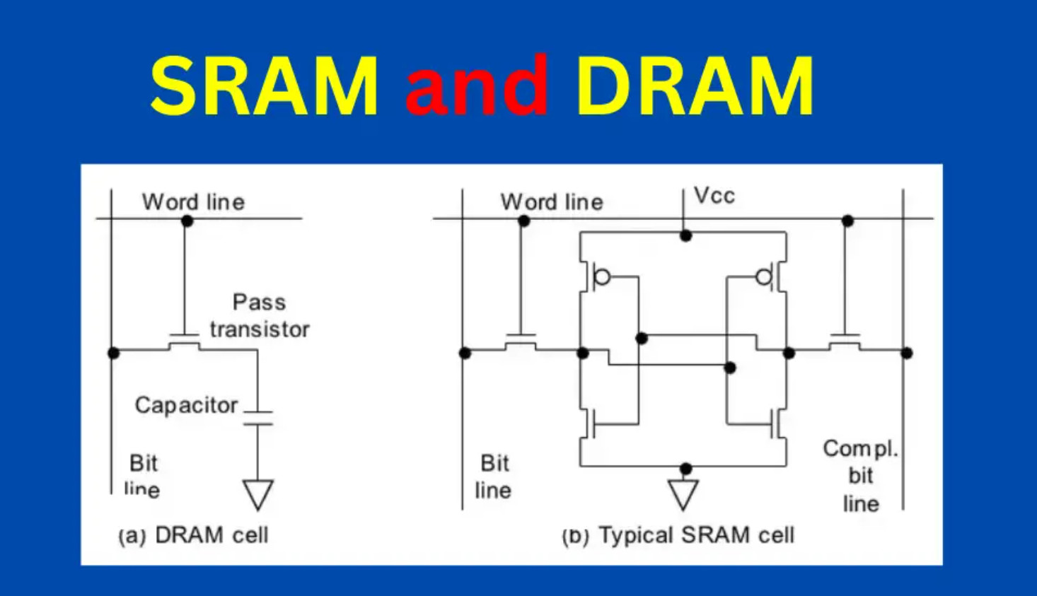
*DRAM Dynamic RAM uses capacitors, slower, cheaper, requires refreshing | |||
*SRAM Static RAM uses transistors, faster<br> | |||
[[File:SRAM vs DRAM.jpg|500px]]<br> | |||
==Types Of Addressing Memory== | |||
These are the types of addressing. | |||
*Random Address (RAM) | |||
*Direct Addressing (HDD) | |||
*Sequential Addressing (Tapes) | |||
*Associative Addressing (Caching) | |||
Speed and Cost Per Bit change goes down as performance goes down. | |||
==Cache Memory== | |||
===Introduction=== | |||
Terms | |||
*Miss Element was not found | |||
*Hit Element was found | |||
*Hit Rate Percentage of time that element was found | |||
Effective Access Time = | |||
Hit Rate * Time from Cache + (1 - Hit rate) - time from Memory | |||
Looking at examples, it was the hit rate that the tutor wanted us to focus on as the other parts would not change.<br> | |||
<br> | |||
For loops indicate to the compiler that we will probably access data more than once and maybe its neighbours. | |||
===Types of Associative Cache=== | |||
There are 3 types of associative addressing cache algorithms | |||
*Fully Associative | |||
*Direct Mapping | |||
*Set Associative | |||
Each of the approaches uses tag value approach where the tag is part of the address and the value is organized to allow to find the element | |||
===Fully Associative=== | |||
For this approach the Full address is split between the Block ID and a number of bits known as the Word ID. The Block ID becomes the Tag. And the value is divided into slots based on the size of the word ID. | |||
*1-bits 2 elements are stored slot-0, slot-1 | |||
*2-bits 4 elements are stored slot-0, slot-1, slot-2,-slot-3 | |||
This is shown below<br> | |||
[[File:Fully Associative.jpg|300px]]<br> | |||
The values are replaced in the case using a replacement alogorthm such as | |||
*FIFO First in First Out | |||
*LRU Least Recently Used. Replaced Block least used | |||
*LFU Least Frequently Used. Replaced Block least frequently used | |||
*Random Just pick one | |||
This approach has the least chance of thrashing but is expensive and slow. | |||
===Direct Mapping=== | |||
For this approach we use the more of the address to store a line ID. | |||
The Full Address is not split into | |||
*Tag first part of address | |||
*Line ID, which line of the cache to store data in | |||
*Word ID, as before the slot for the data in the value | |||
This does not need a replacement algorithm and is therefore fast and cheap. But given the line IDs means data can be replaced often it is prone to thrashing. | |||
===Set Associative=== | |||
This is similar to the above example where instead of a Line ID, a Set ID is stored. I.E. the cache has n rows size of set ID. Shown below is a line ID of 2-bits so each row has two slots. For this approach we do need a replacement algorithm. This approach is used by raspberry PI and many manufacturers<br> | |||
[[File:Set Asscociative.jpg|300px]]<br> | |||
===Flags in Cache=== | |||
Along with tag and value there are flags associated with a row. They are | |||
*Type Data or Instructrion | |||
*Valid Whether valid | |||
*Lock Lock flag | |||
*Dirty bit - Identifies a line of data that has been written to but not been updated | |||
==Memory Device Interface== | ==Memory Device Interface== | ||
Here was shown how the circuit might work with D Flip-Flops and a clock line. Added was an address decoders to allow the device to select the right clock line. Three other signals are required, a write, a read and a chip select.<br> | Here was shown how the circuit might work with D Flip-Flops and a clock line. Added was an address decoders to allow the device to select the right clock line. Three other signals are required, a write, a read and a chip select.<br> | ||
| Line 194: | Line 151: | ||
To maybe see a real world example here is windows showing us the memory map range for a device.<br> | To maybe see a real world example here is windows showing us the memory map range for a device.<br> | ||
[[File:Chip Select Real World.jpeg|700px]]<br> | [[File:Chip Select Real World.jpeg|700px]]<br> | ||
Latest revision as of 22:52, 5 February 2025
Introduction
My knowledge is very small, no not just in general, but on this subject in computers. This is probably where I regret not having a degree. But here goes I am going to try and understand enough of the diagram from the STM32F0xx Cortex-M0 to be dangerous.
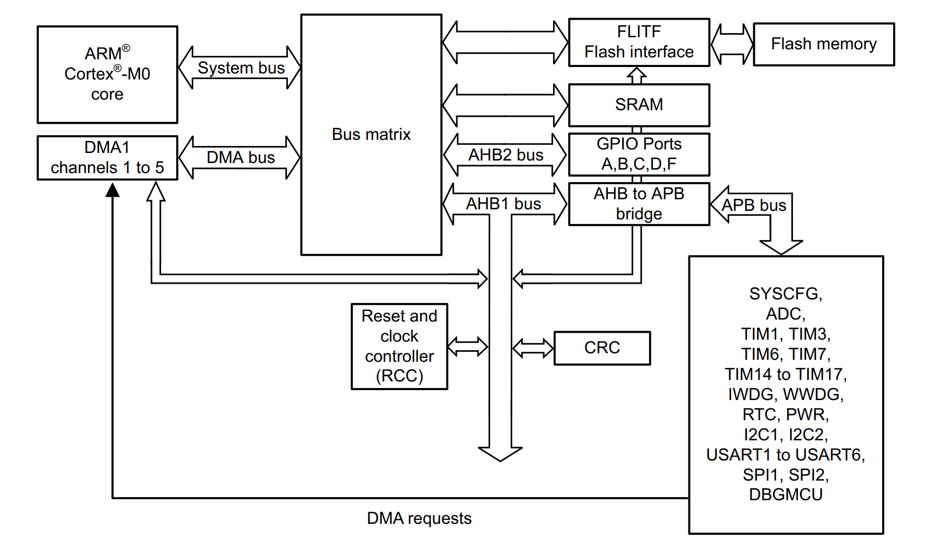
I am again looking at Intermation and their course which is Computer Organization and design.
NVIC and EXTI
Not fully on board with this but the NVIC (Nested Vectored Interrupt Controller) is a interrupt controller connected to the CPU. From one of the docs (STM32G4) it lists its features as
- 102 interrupt sources,
- 16 programmable priority levels,
- Low-latency exception and interrupt handling,
- Automatic nesting,
- Power management control.
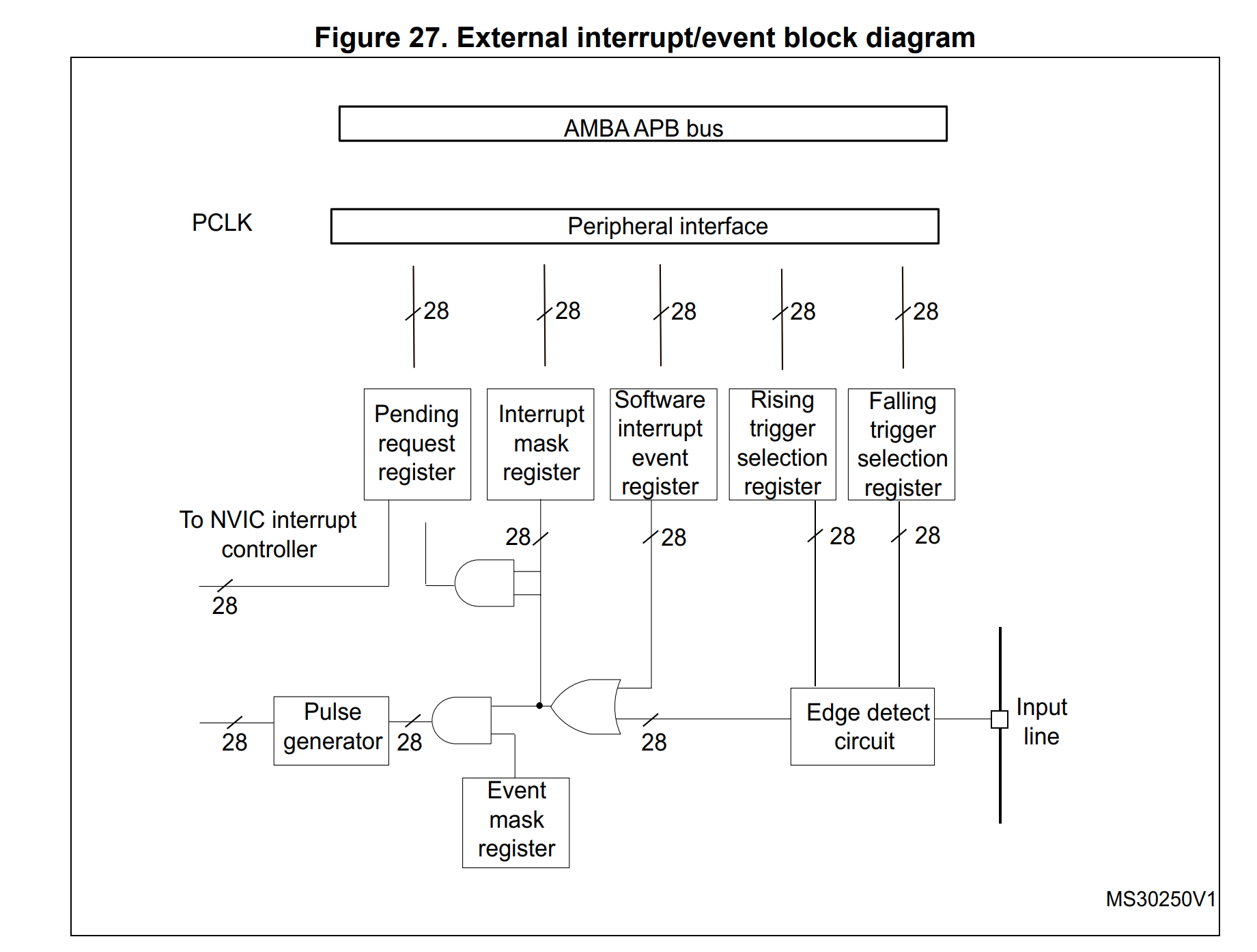
In the lesson I was doing this came up because of the EXTI (EXTernal Interrupt/Event) controller which is connected to the NVIC. When using CubeMX you can configure handlers for the GPIO pin which connects to the EXTI on the NVIC. In my case there are 28 lines on the EXTI
Pending Request Register
When we press a button it is flagged in the pending request register shown above. We can get the address of the register from the manual. In the case of the STM32F302R8 we can first find the EXTI in the manual
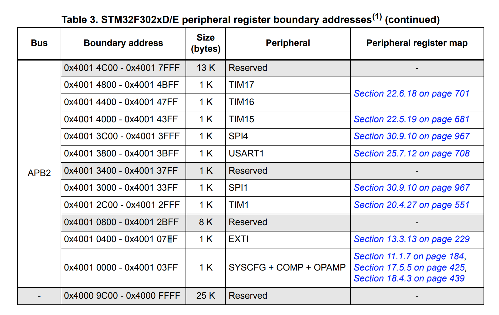
This is probably more about navigating the documentation than the detail but here is the EXTI_PR1 document. After all the software is easy
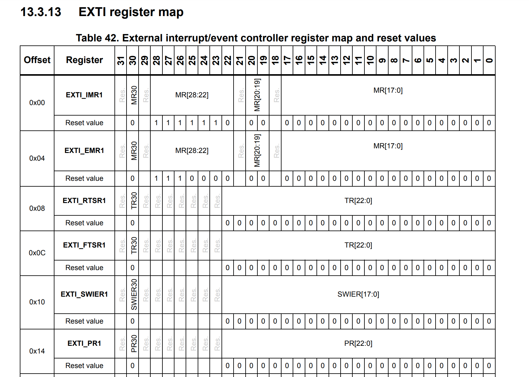
So the address of the EXIT is 0x4001 0400 - 0x4001 07FF and when we look for EXTI_PR1 it is offset 0x14 so the address is 0x4001 0414.
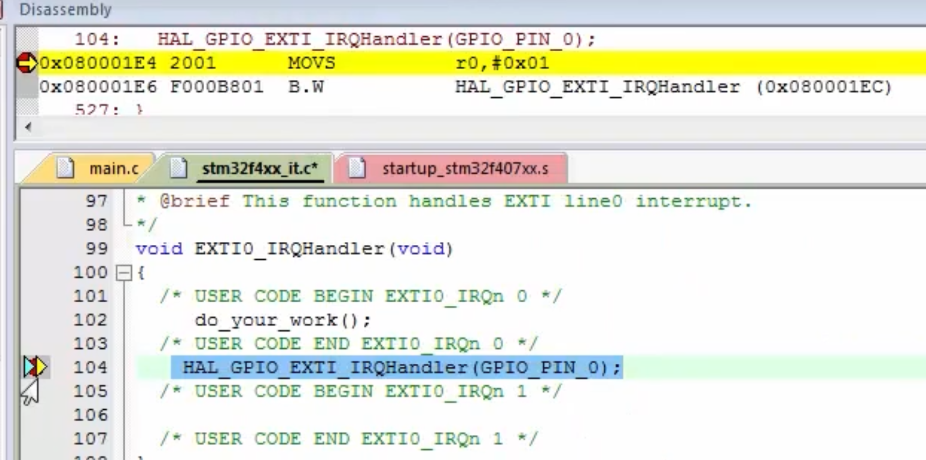
They were very keen to stress that it is the programmers (so old fashioned) job to clear the bit in the PR when done. Using the CubeMX this is what is generated for you via macros.
STM32 Header Files
Briefly ARM have a thing called CMIS. Vendors follow these guidelines and share common macros etc.
Volatile Keyword
Looking at the headers at lot of the headers specify volatile. This forces the compiler to always read the value and not optimize out. With an optimizer the value of p in the code below is not updated and remains in the first loop if the volatile keyword is not used.
#include <stdint.h>


#define SRAM_ADDRESS1   0x20000004U

int main(void)
{

  uint32_t value = 0;
  uint32_t volatile *p = (uint32_t *) SRAM_ADDRESS1;

    while(1)
  {
   value = *p;
   if(value) break;

  }

  while(1);

  return 0;
}
GPIO and Ports
Resetting Ports
Again for documentation most of the STM32 boards will list the peripheral and have the register as the last entry. When you look at the ports some of the reset value might not be neccessarily 0x000 0000. For the STM32F302R8 they were
Address offset:0x00
- Reset value: 0xA800 0000 for port A
- Reset value: 0x0000 0280 for port B
- Reset value: 0x0000 0000 for other ports
Each GPIO should have a pullup resistor. This ensures pins are not floating,neither positive or negative, which will happen due to residual voltage. The pullup resistor value can be found in the documentation searching for Rₚᵤ. or Weak Pull-up.
GPIO Modes
A bit was said about this and the importance of using pullup resistors. The open drain setting was brought up with I2C so may come back to this.
- Input
- Output
- Push/Pull (0 or 1)
- Open Drain (0 or floating)
Speed (Output Only)
We can set the speed of the output using the OSPEEDRy. There are two bits for each port this effect the rising time and falling time. You have to refer to the datasheet (separate from reference manual) to understand the different available speeds. Search for OSPEEDS. I will be very happy if I ever need this. The speed are based on the voltage and clock capacitance.
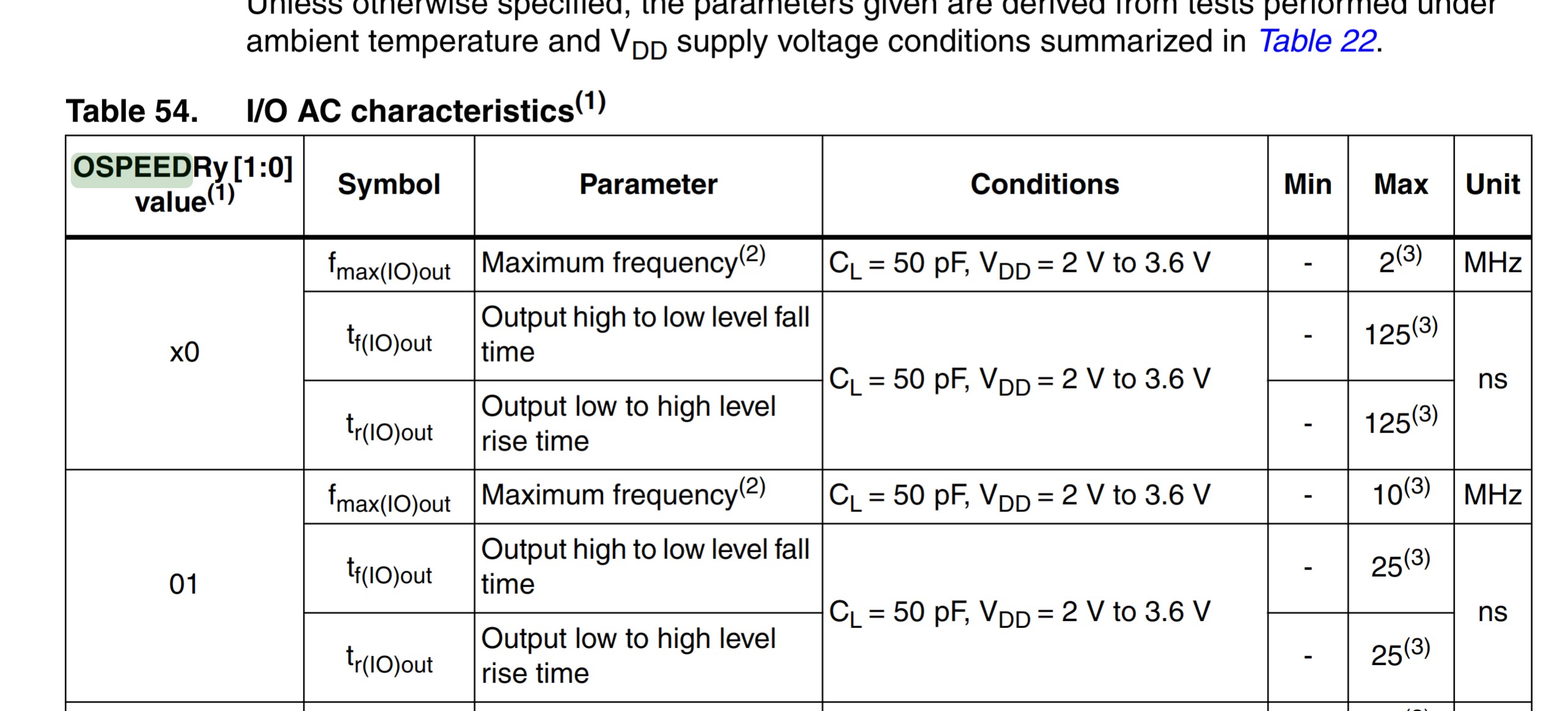
A use case I have heard for setting these speeds is bit-banging which currently I do not understand but believe you could fake an interface by this technique.
The slew rate is defined as the maximum rate of output voltage change per unit time. It is denoted by the letter S. The slew rate helps us to identify the amplitude and maximum input frequency suitable to an operational amplifier (OP amp) such that the output is not significantly distorted.
Alternate Function Mapping
There are 16 different alternate functions pins can be used for. For STM you can generally see this on the pinout when googling but he datasheet also holds a table Alternate Function Mapping showing which pins support what. These can be configured using the Alternate Function Register High (AFRH) and Alternate Function Register Low (AFRL)
Other Stuff
Memory Hierarchy
There is a Hierarchy
- Registers
- Cache (L1 Local, L2 Shared)
- Main Memory (RAM)
- Long Term Storage (Hard Disks, Tapes etc)
Types Of Memory
- DRAM Dynamic RAM uses capacitors, slower, cheaper, requires refreshing
- SRAM Static RAM uses transistors, faster
Types Of Addressing Memory
These are the types of addressing.
- Random Address (RAM)
- Direct Addressing (HDD)
- Sequential Addressing (Tapes)
- Associative Addressing (Caching)
Speed and Cost Per Bit change goes down as performance goes down.
Cache Memory
Introduction
Terms
- Miss Element was not found
- Hit Element was found
- Hit Rate Percentage of time that element was found
Effective Access Time =
   Hit Rate * Time from Cache  + (1 - Hit rate) - time from Memory
Looking at examples, it was the hit rate that the tutor wanted us to focus on as the other parts would not change.
For loops indicate to the compiler that we will probably access data more than once and maybe its neighbours.
Types of Associative Cache
There are 3 types of associative addressing cache algorithms
- Fully Associative
- Direct Mapping
- Set Associative
Each of the approaches uses tag value approach where the tag is part of the address and the value is organized to allow to find the element
Fully Associative
For this approach the Full address is split between the Block ID and a number of bits known as the Word ID. The Block ID becomes the Tag. And the value is divided into slots based on the size of the word ID.
- 1-bits 2 elements are stored slot-0, slot-1
- 2-bits 4 elements are stored slot-0, slot-1, slot-2,-slot-3
This is shown below

The values are replaced in the case using a replacement alogorthm such as
- FIFO First in First Out
- LRU Least Recently Used. Replaced Block least used
- LFU Least Frequently Used. Replaced Block least frequently used
- Random Just pick one
This approach has the least chance of thrashing but is expensive and slow.
Direct Mapping
For this approach we use the more of the address to store a line ID. The Full Address is not split into
- Tag first part of address
- Line ID, which line of the cache to store data in
- Word ID, as before the slot for the data in the value
This does not need a replacement algorithm and is therefore fast and cheap. But given the line IDs means data can be replaced often it is prone to thrashing.
Set Associative
This is similar to the above example where instead of a Line ID, a Set ID is stored. I.E. the cache has n rows size of set ID. Shown below is a line ID of 2-bits so each row has two slots. For this approach we do need a replacement algorithm. This approach is used by raspberry PI and many manufacturers

Flags in Cache
Along with tag and value there are flags associated with a row. They are
- Type Data or Instructrion
- Valid Whether valid
- Lock Lock flag
- Dirty bit - Identifies a line of data that has been written to but not been updated
Memory Device Interface
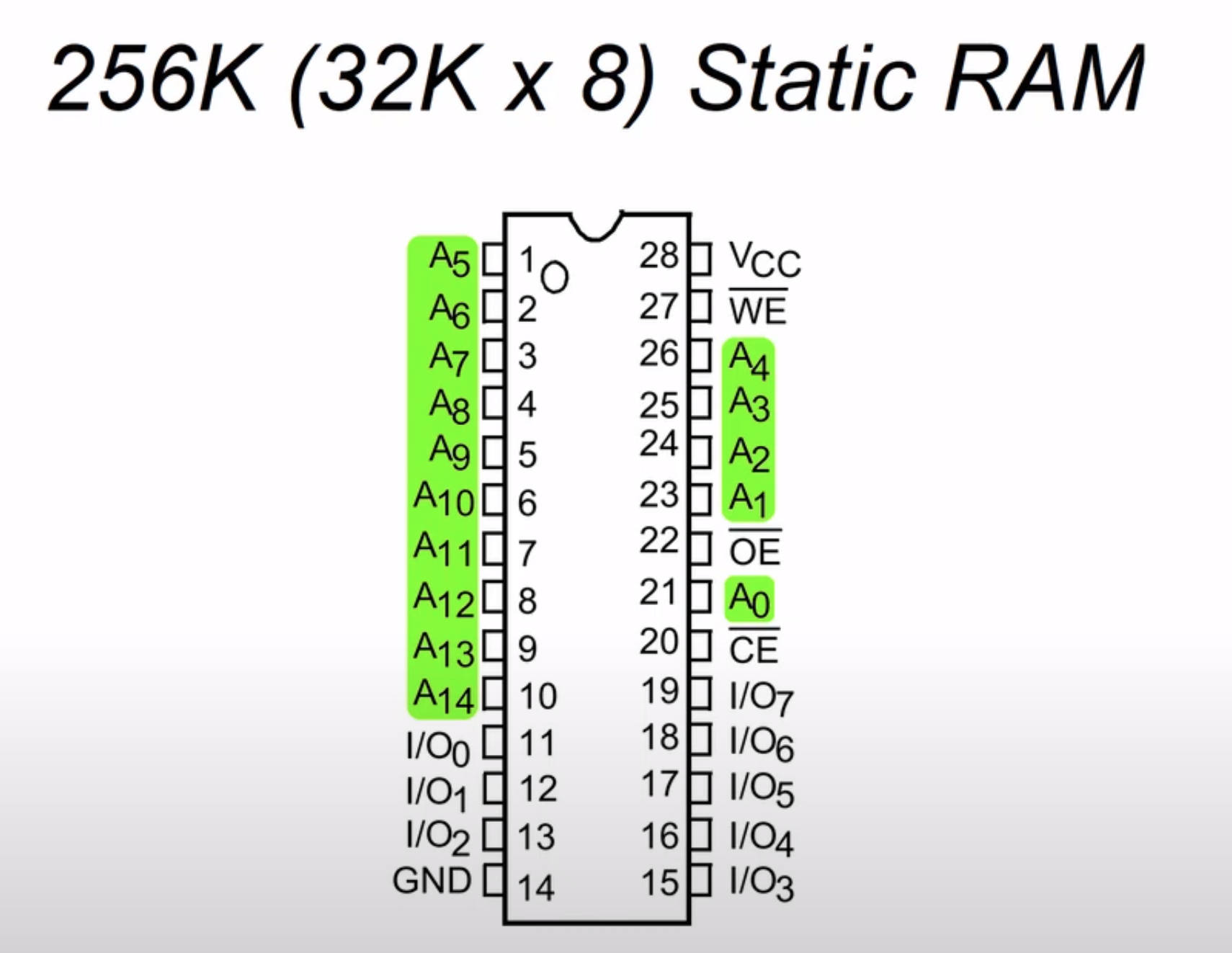
Here was shown how the circuit might work with D Flip-Flops and a clock line. Added was an address decoders to allow the device to select the right clock line. Three other signals are required, a write, a read and a chip select.

Ironically he went on to show this device which I reckon is the one I am using for the 6502.
Chip Select
When we look at an MCU there is a memory map which shows where the peripherals are on the device. Each device has a range of memory used to operate it.
There are address lines within the mcu which are connected to the device. In the example below there are 20 address lines and the Graphic Card is located between 0xE0000 and 0xFFFFF. Putting this number into binary shows that address lines A19-A17 is the CS (Chip Select) and address line A16-A00 is the graphic card. Setting A19-A17 to binary 111 effectively means you are using the address lines for the graphics card.

In order to operate the correct memory device from the processor you use the correct chip select.
To maybe see a real world example here is windows showing us the memory map range for a device.

