STM32 Driver Creation: Difference between revisions
Created page with "=STM32 Driver Creation= ==Introduction== This is the start of creating a driver. This is the introd slide where they explained the next few steps.<br> 800px<br> ==Creating a Device Specific Driver File== This is creating a header file which will contain the necessary headers for the peripherals and used in the Application. They suggested this should contain.<br> 600px<br> ===Memory Addresses=== Created..." |
No edit summary |
||
| Line 1: | Line 1: | ||
=Introduction= | |||
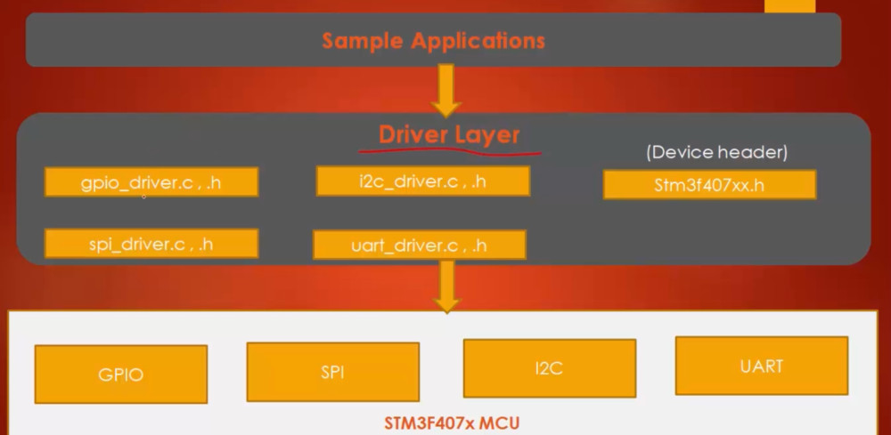
This is the start of creating a driver. This is the introd slide where they explained the next few steps.<br> | This is the start of creating a driver. This is the introd slide where they explained the next few steps.<br> | ||
[[File:STM32 Driver Creation.jpg| 800px]]<br> | [[File:STM32 Driver Creation.jpg| 800px]]<br> | ||
=Creating a Device Specific Driver File= | |||
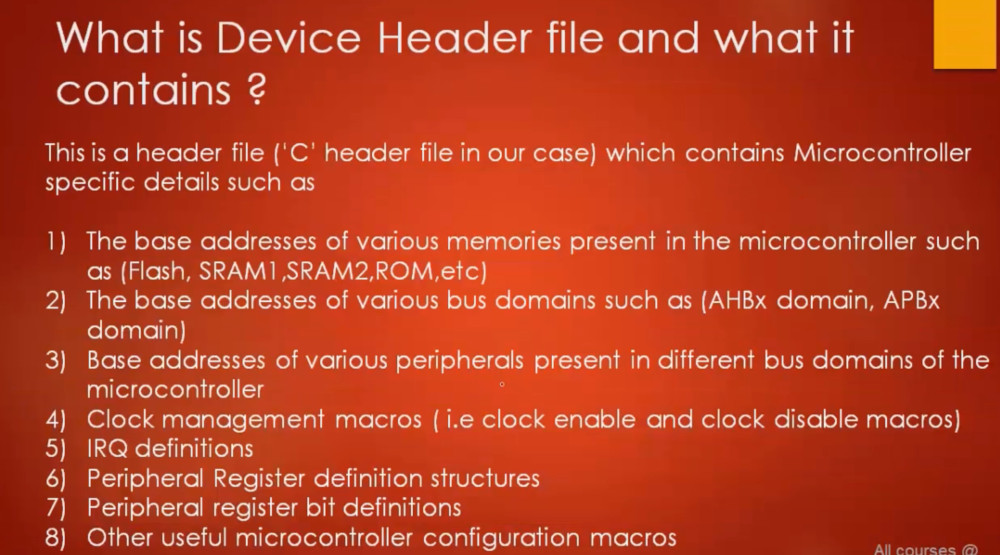
This is creating a header file which will contain the necessary headers for the peripherals and used in the Application. They suggested this should contain.<br> | This is creating a header file which will contain the necessary headers for the peripherals and used in the Application. They suggested this should contain.<br> | ||
[[File:STM32 Driver Header.jpg| 600px]]<br> | [[File:STM32 Driver Header.jpg| 600px]]<br> | ||
==Memory Addresses== | |||
Created a header adding addresses from the controller | Created a header adding addresses from the controller | ||
<syntaxhighlight lang="c"> | <syntaxhighlight lang="c"> | ||
| Line 25: | Line 24: | ||
#endif | #endif | ||
</syntaxhighlight> | </syntaxhighlight> | ||
==Bus Domains== | |||
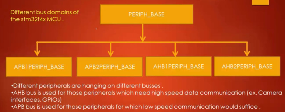
Next we move on the the Bus domains<br> | Next we move on the the Bus domains<br> | ||
[[File:STM32 Bus Domains.jpg|600px]]<br> | [[File:STM32 Bus Domains.jpg|600px]]<br> | ||
| Line 85: | Line 84: | ||
Note the USARTx and UARTx. UARTx do not support synchronous communication. They cannot use the serial (output) clock. | Note the USARTx and UARTx. UARTx do not support synchronous communication. They cannot use the serial (output) clock. | ||
==Registers== | |||
Next the Registers<br> | Next the Registers<br> | ||
[[File:STM32 Register Definitions.jpg|600px]]<br> | [[File:STM32 Register Definitions.jpg|600px]]<br> | ||
| Line 144: | Line 143: | ||
</syntaxhighlight> | </syntaxhighlight> | ||
==Macros Enable/Disable== | |||
===Enable=== | |||
To enable a bit we use the or operator and shift 1 into the specified bit position | To enable a bit we use the or operator and shift 1 into the specified bit position | ||
( address |= ( '''value''' << '''position''' ) | ( address |= ( '''value''' << '''position''' ) | ||
| Line 153: | Line 152: | ||
#define ENABLE_THIS (RCC->APB2ENR |= (1 << 12)) | #define ENABLE_THIS (RCC->APB2ENR |= (1 << 12)) | ||
</syntaxhighlight> | </syntaxhighlight> | ||
===Disable=== | |||
To disable a bit we use the and operator and negated shift 1 into the specified bit position | To disable a bit we use the and operator and negated shift 1 into the specified bit position | ||
( address &= ~( '''value''' << '''position''' ) | ( address &= ~( '''value''' << '''position''' ) | ||
| Line 218: | Line 217: | ||
</syntaxhighlight> | </syntaxhighlight> | ||
=GPIO Driver File= | |||
Next we create a file defining the API for GPIO we will support and structures to support it | Next we create a file defining the API for GPIO we will support and structures to support it | ||
<syntaxhighlight lang="c"> | <syntaxhighlight lang="c"> | ||
| Line 244: | Line 243: | ||
number ^= 1 << x; | number ^= 1 << x; | ||
</syntaxhighlight> | </syntaxhighlight> | ||
=IRQs= | |||
==Introduction== | |||
The is how to handle IRQs for the STM32 devices. So far we have slide which I need to add more comments.<br> | The is how to handle IRQs for the STM32 devices. So far we have slide which I need to add more comments.<br> | ||
[[File:STM32 IRQ Overview.jpg|500px]]<br> | [[File:STM32 IRQ Overview.jpg|500px]]<br> | ||
| Line 254: | Line 253: | ||
*Vector table hold information 23 and 40 | *Vector table hold information 23 and 40 | ||
At the time they mentioned the Peripheral side vs Processor side. What they meant was the non-chip side. I.E. the part provided by STM32 and the part provided by ARM Cortex m4<br> | At the time they mentioned the Peripheral side vs Processor side. What they meant was the non-chip side. I.E. the part provided by STM32 and the part provided by ARM Cortex m4<br> | ||
==Actual Steps== | |||
The video seem to make its own names for dithered on what the steps are. I am going to do the same using my own point of view | The video seem to make its own names for dithered on what the steps are. I am going to do the same using my own point of view | ||
*Configure The Edge Trigger RT, FT and RFT (Peripheral Side) | *Configure The Edge Trigger RT, FT and RFT (Peripheral Side) | ||
| Line 264: | Line 263: | ||
*Implement Override IRQ Handler (Application) | *Implement Override IRQ Handler (Application) | ||
==Configure GPIO Pin== | |||
Here are the steps to configuring the GPIO Pins based on the video<br> | Here are the steps to configuring the GPIO Pins based on the video<br> | ||
[[File:STM32 IRQ2 Overview.jpg|500px]]<br> | [[File:STM32 IRQ2 Overview.jpg|500px]]<br> | ||
===Configure The Edge Trigger RT, FT and RFT (Peripheral Side)=== | |||
So we need to create the structures similar to RCC to hold EXTI and SYSCFG in the driver | So we need to create the structures similar to RCC to hold EXTI and SYSCFG in the driver | ||
<syntaxhighlight lang="c"> | <syntaxhighlight lang="c"> | ||
| Line 326: | Line 325: | ||
</syntaxhighlight> | </syntaxhighlight> | ||
===Enable Delivery from the Peripheral to the Processor (Peripheral Side)=== | |||
Carrying on in GPIO_Init we set the Port in the EXICR (EXTI Configuration Register). For our device the are four of these. | Carrying on in GPIO_Init we set the Port in the EXICR (EXTI Configuration Register). For our device the are four of these. | ||
<syntaxhighlight lang="c"> | <syntaxhighlight lang="c"> | ||
| Line 346: | Line 345: | ||
</syntaxhighlight> | </syntaxhighlight> | ||
===Identify the EXTI Line based on the GPIO Pin Number=== | |||
The EXTI Lines connections are specific to the Micro-controller families. For the ST32F4xx it is | The EXTI Lines connections are specific to the Micro-controller families. For the ST32F4xx it is | ||
<syntaxhighlight lang="c"> | <syntaxhighlight lang="c"> | ||
| Line 368: | Line 367: | ||
</syntaxhighlight> | </syntaxhighlight> | ||
===Configure Priority (Processor Side)=== | |||
The key thing was to understand the memory layout and that the Number of Priority Bit differs from chip manufacturer and maybe even MCU. For the cortex M4 there are 60 registers with 32 bits.<br> | The key thing was to understand the memory layout and that the Number of Priority Bit differs from chip manufacturer and maybe even MCU. For the cortex M4 there are 60 registers with 32 bits.<br> | ||
[[File:PR Register.jpg|300px]]<br> | [[File:PR Register.jpg|300px]]<br> | ||
| Line 387: | Line 386: | ||
</syntaxhighlight> | </syntaxhighlight> | ||
===Set Enable/Clear Register for IRQ (Processor Side)=== | |||
To enable/disable the IRQ we need to enable the correct NVIC_ISER or NVIC_ICER. In the driver header we set these at the top. These addresses can be found in the Cortex m4. | To enable/disable the IRQ we need to enable the correct NVIC_ISER or NVIC_ICER. In the driver header we set these at the top. These addresses can be found in the Cortex m4. | ||
<syntaxhighlight lang="c"> | <syntaxhighlight lang="c"> | ||
| Line 442: | Line 441: | ||
</syntaxhighlight> | </syntaxhighlight> | ||
===Clear EXTI PR Register for GPIO Pin (Peripheral Side)=== | |||
When we want to implement an IRQ handler we need to clear the EXIT PR register by writing 1 for that GPIO pin | When we want to implement an IRQ handler we need to clear the EXIT PR register by writing 1 for that GPIO pin | ||
<syntaxhighlight lang="c"> | <syntaxhighlight lang="c"> | ||
| Line 458: | Line 457: | ||
} | } | ||
</syntaxhighlight> | </syntaxhighlight> | ||
===Implement Override IRQ Handler (Application)=== | |||
Implementing the handler is the easiest part. Default handlers are provided in the .s file provided with the board and run at startup. In the startup code in the .s you will see | Implementing the handler is the easiest part. Default handlers are provided in the .s file provided with the board and run at startup. In the startup code in the .s you will see | ||
<syntaxhighlight lang="c"> | <syntaxhighlight lang="c"> | ||
| Line 471: | Line 470: | ||
} | } | ||
</syntaxhighlight> | </syntaxhighlight> | ||
=SPI= | |||
Next we are looking at SPI. Below is a list of possible protocols and usage for MCUs<br> | Next we are looking at SPI. Below is a list of possible protocols and usage for MCUs<br> | ||
[[File:Protocol Types.jpg|500px]]<br> | [[File:Protocol Types.jpg|500px]]<br> | ||
There are 3 SPI modes. These are shown below. Some SPI devices might not support all.<br> | There are 3 SPI modes. These are shown below. Some SPI devices might not support all.<br> | ||
[[File:SPI Modes.jpeg|500px]]<br> | [[File:SPI Modes.jpeg|500px]]<br> | ||
==NSS Slave Select Management== | |||
On the slave we can manage the NSS pin for SPI using the SPIx_CR1 register for STM32. This allow us, when SSM=1, to ground the state via the SSI value, SSI=0 is grounded, SSI=1 is pulled high. This frees up the NSS pin for other usage. Otherwise we need to ground this pin. | On the slave we can manage the NSS pin for SPI using the SPIx_CR1 register for STM32. This allow us, when SSM=1, to ground the state via the SSI value, SSI=0 is grounded, SSI=1 is pulled high. This frees up the NSS pin for other usage. Otherwise we need to ground this pin. | ||
<br> | <br> | ||
Where there are multiple slaves you would not use the NSS pin and '''this would be tied to vdd (high)'''. Separate pins would be used instead for each slave so they can be used independantly.<br> | Where there are multiple slaves you would not use the NSS pin and '''this would be tied to vdd (high)'''. Separate pins would be used instead for each slave so they can be used independantly.<br> | ||
[[File:SPI Multiple.jpeg|400px]] | [[File:SPI Multiple.jpeg|400px]] | ||
==Communication format== | |||
We need to be aware of | We need to be aware of | ||
*SCLK Phase (CPHA) | *SCLK Phase (CPHA) | ||
| Line 489: | Line 488: | ||
[[File:CPOL CPHA.jpeg|400px]]<br> | [[File:CPOL CPHA.jpeg|400px]]<br> | ||
You will need to check the documentation of which mode CPHA/CPOL and device can be configured to.<br> | You will need to check the documentation of which mode CPHA/CPOL and device can be configured to.<br> | ||
==Clocks== | |||
For STM32 there is a HCLK which is the hardware clock. There is a prescaler which divides the clock between the HCLK and the bus.<br> | For STM32 there is a HCLK which is the hardware clock. There is a prescaler which divides the clock between the HCLK and the bus.<br> | ||
[[File:STM32 Clocks.jpeg| 200]]<br> | [[File:STM32 Clocks.jpeg| 200]]<br> | ||
| Line 496: | Line 495: | ||
Here is an example of the SPI clock for the course. Because we are using HSI clock the speed is 16Hhz if we used a different clock it could be 42 Mhz. This means the max speed, if using the faster clock could be 21Mhz. In this case we are using 16Hhz so 8Mhz is the speed.<br> | Here is an example of the SPI clock for the course. Because we are using HSI clock the speed is 16Hhz if we used a different clock it could be 42 Mhz. This means the max speed, if using the faster clock could be 21Mhz. In this case we are using 16Hhz so 8Mhz is the speed.<br> | ||
[[File:STM32 SPI Example Clock.jpeg | 300px]]<br> | [[File:STM32 SPI Example Clock.jpeg | 300px]]<br> | ||
=Driver Changes= | |||
==General== | |||
We need to define the register map for SPI using the reference manual | We need to define the register map for SPI using the reference manual | ||
<syntaxhighlight lang="c"> | <syntaxhighlight lang="c"> | ||
| Line 555: | Line 554: | ||
#endif | #endif | ||
</syntaxhighlight> | </syntaxhighlight> | ||
==APIs== | |||
We can use some of the definitions from the GPIO APIs but we do need to define the send and receive functions | We can use some of the definitions from the GPIO APIs but we do need to define the send and receive functions | ||
<syntaxhighlight lang="c"> | <syntaxhighlight lang="c"> | ||
| Line 589: | Line 588: | ||
#define SPI_BUS_CONFIG_SIMPLEX_RXONLY 3 | #define SPI_BUS_CONFIG_SIMPLEX_RXONLY 3 | ||
</syntaxhighlight> | </syntaxhighlight> | ||
==Send Data== | |||
Here is the logic around the send data. Hopefully looking back this will make sense on how to handle 8-bit/16-bit etc. Again co-pilot could get an implementation from the web<br> | Here is the logic around the send data. Hopefully looking back this will make sense on how to handle 8-bit/16-bit etc. Again co-pilot could get an implementation from the web<br> | ||
[[File:STM32 SPI SendData.jpeg|400px]]<br> | [[File:STM32 SPI SendData.jpeg|400px]]<br> | ||
| Line 624: | Line 623: | ||
} | } | ||
</syntaxhighlight> | </syntaxhighlight> | ||
==Receive Data== | |||
So here is the receive data. It should be getting easier now<br> | So here is the receive data. It should be getting easier now<br> | ||
[[File:STM32 SPI Receive Data.jpg|400px]]<br> | [[File:STM32 SPI Receive Data.jpg|400px]]<br> | ||
| Line 630: | Line 629: | ||
</syntaxhighlight> | </syntaxhighlight> | ||
==Testing== | |||
We can use PulseView and a logic analyzer to test this. I had to build the software from scratch on Ubuntu 23.04. Without this then there are no drivers. I did update the udev rules for Saleae so this could be run without root. | We can use PulseView and a logic analyzer to test this. I had to build the software from scratch on Ubuntu 23.04. Without this then there are no drivers. I did update the udev rules for Saleae so this could be run without root. | ||
<syntaxhighlight lang="txt"> | <syntaxhighlight lang="txt"> | ||
Latest revision as of 22:50, 5 February 2025
Introduction
This is the start of creating a driver. This is the introd slide where they explained the next few steps.
Creating a Device Specific Driver File
This is creating a header file which will contain the necessary headers for the peripherals and used in the Application. They suggested this should contain.
Memory Addresses
Created a header adding addresses from the controller
#ifndef __stm32F302__h
#define __stm32F302__h

/*
 * Base address of Flash and RAM
 * Note we can either cast to (uint32_t) or add a U to denote
 * unsigned to the compiler
 * SROM is labelled System Memory in the Reference Manual
 */

#define FLASH_BASEADDR  0x08000000U
#define SRAM1_BASEADDR  0x20000000U
#define SRAM            SRAM1_BASEADDR
#define ROM_BASEADDR    0x1FFFD800U
#endif
Bus Domains
Next we move on the the Bus domains
...
/*
 * AHBx and APBx Bus Peripheral Base Address
 * These were list in reverse order in the
 * Reference manual
 */

#define AHB3PERIPH_BASE 0x50000000U
#define AHB2PERIPH_BASE 0x48000000U
#define AHB1PERIPH_BASE 0x40020000U
#define APB2PERIPH_BASE 0x40010000U
#define APB1PERIPH_BASE 0x40000000U
Peripherals
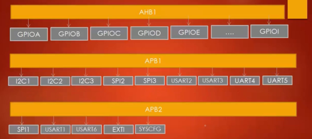
And now the actual peripherals
...
/*
 * Base address of all hanging off AHB1
 */
#define RCC_BASEADDR    (AHB1PERIPH_BASE + 0x1000)

/*
 * Base address of all hanging off AHB2
 */
#define GPIOA_BASEADDR  (AHB2PERIPH_BASE + 0x0000)
#define GPIOB_BASEADDR  (AHB2PERIPH_BASE + 0x0400)
#define GPIOC_BASEADDR  (AHB2PERIPH_BASE + 0x0800)
#define GPIOD_BASEADDR  (AHB2PERIPH_BASE + 0x0C00)
#define GPIOE_BASEADDR  (AHB2PERIPH_BASE + 0x1000)
#define GPIOF_BASEADDR  (AHB2PERIPH_BASE + 0x1400)

/*
 * Base address of all hanging off APB1
 */
#define SPI2_BASEADDR    (APB1PERIPH_BASE + 0x3800)
#define SPI3_BASEADDR    (APB1PERIPH_BASE + 0x3C00)
#define USART2_BASEADDR  (APB1PERIPH_BASE + 0x4400)
#define USART3_BASEADDR  (APB1PERIPH_BASE + 0x4800)
#define UART4_BASEADDR   (APB1PERIPH_BASE + 0x4C00)
#define UART5_BASEADDR   (APB1PERIPH_BASE + 0x5000)
#define I2C1_BASEADDR    (APB1PERIPH_BASE + 0x5400)
#define I2C2_BASEADDR    (APB1PERIPH_BASE + 0x5800)

/*
 * Base address of all hanging off APB2
 */
#define SYSCFG_BASEADDR    (APB2PERIPH_BASE + 0x0000)
#define EXTI_BASEADDR      (APB2PERIPH_BASE + 0x0400)
#define SPI1_BASEADDR      (APB2PERIPH_BASE + 0x3000)
#define USART1_BASEADDR    (APB2PERIPH_BASE + 0x3800)
Note the USARTx and UARTx. UARTx do not support synchronous communication. They cannot use the serial (output) clock.
Registers
Next the Registers
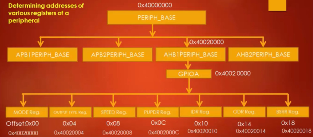
We look in the Reference Manual under GPIO register map and we map their structure in a C struct.
...
/* GPIO Register Map */
typedef struct {

    volatile uint32_t MODER;
    volatile uint32_t OTYPER;
    volatile uint32_t OSPEEDR;
    volatile uint32_t PUPDR;
    volatile uint32_t IDR;
    volatile uint32_t ODR;
    volatile uint32_t BSRR;
    volatile uint32_t LCKR;
    volatile uint32_t AFR[2];

} GPIO_RegDef_t;
Now the RCC Register
...
/* RCC Register Map */
typedef struct {

    volatile uint32_t CR;
    volatile uint32_t CFGR;
    volatile uint32_t CIR;
    volatile uint32_t APB2RSTR;
    volatile uint32_t APB1RSTR;
    volatile uint32_t APB2ENR;
    volatile uint32_t APB1ENR;
    volatile uint32_t BDCR;
    volatile uint32_t CSR;
    volatile uint32_t AHBRSTR;
    volatile uint32_t CFGR2;
    volatile uint32_t CFGR3;

} RCC_RegDef_t;
...
And now the peripherals
/* Peripheral Addresses */
#define GPIOA             ((GPIO_RegDef_t*)(GPIOA_BASEADDR))
#define GPIOB             ((GPIO_RegDef_t*)(GPIOB_BASEADDR))
#define GPIOC             ((GPIO_RegDef_t*)(GPIOC_BASEADDR))
#define GPIOD             ((GPIO_RegDef_t*)(GPIOD_BASEADDR))
#define GPIOE             ((GPIO_RegDef_t*)(GPIOE_BASEADDR))
#define GPIOF             ((GPIO_RegDef_t*)(GPIOF_BASEADDR))

#define RCC               ((RCC_RegDef_t*)(RCC_BASEADDR))
#define EXI               ((RCC_RegDef_t*)(EXTI_BASEADDR))
...
Macros Enable/Disable
Enable
To enable a bit we use the or operator and shift 1 into the specified bit position
( address |= ( value << position )
For example to set a 1 in RCC->APB2ENR bit 12
#define ENABLE_THIS (RCC->APB2ENR |= (1 << 12))
Disable
To disable a bit we use the and operator and negated shift 1 into the specified bit position
( address &= ~( value << position )
For example to set a 0 in RCC->APB2ENR bit 12
#define DISABLE_THIS (RCC->APB2ENR &= ~(1 << 12))
And here are the macros for the peripherals above
...
/* Clock Enable Macros for GPIOx peripherals */
#define GPIOA_PCLK_EN() (RCC->AHBENR |= (1 << 17))
#define GPIOB_PCLK_EN() (RCC->AHBENR |= (1 << 18))
#define GPIOC_PCLK_EN() (RCC->AHBENR |= (1 << 19))
#define GPIOD_PCLK_EN() (RCC->AHBENR |= (1 << 20))
#define GPIOE_PCLK_EN() (RCC->AHBENR |= (1 << 21))
#define GPIOF_PCLK_EN() (RCC->AHBENR |= (1 << 22))

/* Clock Enable Macros for I2Cx peripherals */
#define I2C1_PCLK_EN() (RCC->APB1ENR |= (1 << 21))
#define I2C2_PCLK_EN() (RCC->APB1ENR |= (1 << 22))

/* Clock Enable Macros for SPIx peripherals */
#define SPI2_PCLK_EN() (RCC->APB1ENR |= (1 << 14))
#define SPI3_PCLK_EN() (RCC->APB1ENR |= (1 << 15))
#define SPI1_PCLK_EN() (RCC->APB2ENR |= (1 << 12))

/* Clock Enable Macros for USARTx peripherals */
#define USART1_PCLK_EN() (RCC->AHB2ENR |= (1 << 14))
#define USART2_PCLK_EN() (RCC->AHB1ENR |= (1 << 17))
#define USART3_PCLK_EN() (RCC->AHB1ENR |= (1 << 18))

/* Clock Enable Macros for SYSCFG peripherals */
#define SYSCFG_PCLK_EN() (RCC->AHB1ENR |= (1 << 0))


/* Clock Disable Macros for GPIOx peripherals */
#define GPIOA_PCLK_DI() (RCC->AHB1ENR &= ~(1 << 17))
#define GPIOB_PCLK_DI() (RCC->AHB1ENR &= ~(1 << 18))
#define GPIOC_PCLK_DI() (RCC->AHB1ENR &= ~(1 << 19))
#define GPIOD_PCLK_DI() (RCC->AHB1ENR &= ~(1 << 20))
#define GPIOE_PCLK_DI() (RCC->AHB1ENR &= ~(1 << 21))
#define GPIOF_PCLK_DI() (RCC->AHB1ENR &= ~(1 << 22))

/* Clock Disable Macros for I2Cx peripherals */
#define I2C1_PCLK_DI() (RCC->APB1ENR &= ~(1 << 21))
#define I2C2_PCLK_DI() (RCC->APB1ENR &= ~(1 << 22))


/* Clock Disable Macros for SPIx peripherals */
#define SPI1_PCLK_DI() (RCC->APB2ENR &= ~(1 << 12))
#define SPI2_PCLK_DI() (RCC->APB1ENR &= ~(1 << 14))
#define SPI3_PCLK_DI() (RCC->APB1ENR &= ~(1 << 15))


/* Clock Disable Macros for USARTx peripherals */
#define USART1_PCLK_DI() (RCC->AHB2ENR &= ~(1 << 14))
#define USART2_PCLK_DI() (RCC->AHB1ENR &= ~(1 << 17))
#define USART3_PCLK_DI() (RCC->AHB1ENR &= ~(1 << 18))

/* Clock Disable Macros for SYSCFG peripherals */
#define SYSCFG_PCLK_DI() (RCC->AHB1ENR &= ~(1 << 0))
GPIO Driver File
Next we create a file defining the API for GPIO we will support and structures to support it
There was lots of functions but main it was about reading, setting and clearing bits.
- Setting a bit
Use the bitwise OR operator (|) to set a bit.
number |= 1 << x;
That will set a bit x.
- Clearing a bit
Use the bitwise AND operator (&) to clear a bit.
number &= ~(1 << x);
That will clear bit x. You must invert the bit string with the bitwise NOT operator (~), then AND it.
- Toggling a bit
The XOR operator (^) can be used to toggle a bit.
number ^= 1 << x;
IRQs
Introduction
The is how to handle IRQs for the STM32 devices. So far we have slide which I need to add more comments.
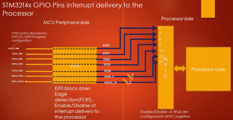
- IRQs disabled by default
- Set the GPIO port to use
- Lines 5-9 are connected to 23
- Lines 10-15 are connected to 40
- Vector table hold information 23 and 40
At the time they mentioned the Peripheral side vs Processor side. What they meant was the non-chip side. I.E. the part provided by STM32 and the part provided by ARM Cortex m4
Actual Steps
The video seem to make its own names for dithered on what the steps are. I am going to do the same using my own point of view
- Configure The Edge Trigger RT, FT and RFT (Peripheral Side)
- Enable Delivery from the Peripheral to the Processor (Peripheral Side)
- Identify the EXTI Line based on the GPIO Pin Number (Peripheral Side)
- Configure Priority (Processor Side)
- Set Enable/Clear Register for IRQ (Processor Side)
- Clear EXTI PR Register for GPIO Pin (Peripheral Side)
- Implement Override IRQ Handler (Application)
Configure GPIO Pin
Here are the steps to configuring the GPIO Pins based on the video
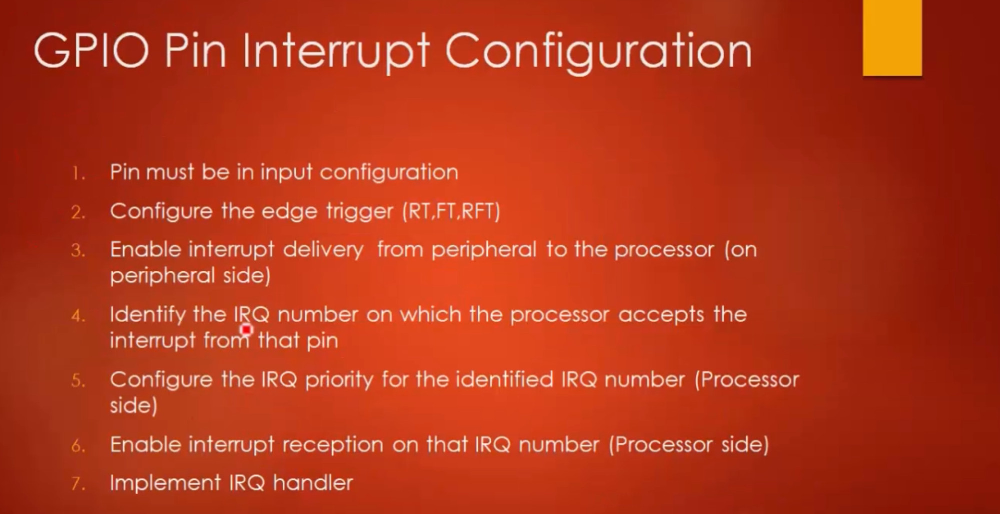
Configure The Edge Trigger RT, FT and RFT (Peripheral Side)
So we need to create the structures similar to RCC to hold EXTI and SYSCFG in the driver
/* EXI Register Map */
typedef struct {
    volatile uint32_t IMR;
    volatile uint32_t EMR;
    volatile uint32_t RTSR;
    volatile uint32_t FTSR;
    volatile uint32_t SWIER;
    volatile uint32_t PR;
    volatile uint32_t RESERVED1;
    volatile uint32_t RESERVED2;
    volatile uint32_t IMR2;
    volatile uint32_t EMR2;
    volatile uint32_t RTSR2;
    volatile uint32_t FTSR2;
    volatile uint32_t SWIER2;
    volatile uint32_t PR2;
} EXTI_RegDef_t;

/* SYSCFG Register Map */
typedef struct {
    volatile uint32_t CFGR1;
    volatile uint32_t EXTICR[4];
    volatile uint32_t CFGR2;
} SYSCFG_RegDef_t;
Now in the GPIO_Init function we configure the edge trigger. When setting one trigger we clear the other to ensure consistency.
void GPIO_Init(GPIO_Handle_t *pGPIOHandle) {
...
        if (pGPIOHandle->GPIO_PinConfig.GPIO_PinMode == GPIO_MODE_IT_FT)
        {
            // 1. Configure FTSR
            // Set bit for FTSR
            EXTI->FTSR |= (1 << pGPIOHandle->GPIO_PinConfig.GPIO_PinNumber);
            // Clear bit for RTSR
            EXTI->RTSR &= ~(1 << pGPIOHandle->GPIO_PinConfig.GPIO_PinNumber);
        }

        else if (pGPIOHandle->GPIO_PinConfig.GPIO_PinMode == GPIO_MODE_IT_RT)
        {

            // Set bit for RTSR
            EXTI->RTSR |= (1 << pGPIOHandle->GPIO_PinConfig.GPIO_PinNumber);
            // Clear bit for FTSR
            EXTI->FTSR &= ~(1 << pGPIOHandle->GPIO_PinConfig.GPIO_PinNumber);
        }
        else if (pGPIOHandle->GPIO_PinConfig.GPIO_PinMode == GPIO_MODE_IT_RFT)
        {

            // 1. Configure FTSR and RFSR
            EXTI->FTSR |= (1 << pGPIOHandle->GPIO_PinConfig.GPIO_PinNumber);
            EXTI->RTSR |= (1 << pGPIOHandle->GPIO_PinConfig.GPIO_PinNumber);
        }
...
Enable Delivery from the Peripheral to the Processor (Peripheral Side)
Carrying on in GPIO_Init we set the Port in the EXICR (EXTI Configuration Register). For our device the are four of these.
void GPIO_Init(GPIO_Handle_t *pGPIOHandle) {
...
        // 2. Configure the GPIO port selection in SYSCFG_EXICR
        uint8_t extiIndex = pGPIOHandle->GPIO_PinConfig.GPIO_PinNumber / 4;
        uint8_t extiPosition = pGPIOHandle->GPIO_PinConfig.GPIO_PinNumber % 4; // Remainder
        uint8_t portCode = GPIO_BASEADDR_TO_CODE(pGPIOHandle->pGPIOx);

        // Enable Clock
        SYSCFG_PCLK_EN();
        uint32_t value = portCode << (extiPosition * 4);
        SYSCFG->EXTICR[extiIndex] = value;

        // 3. Enable the EXI Interrupt delivery using IMR
        EXTI->IMR |= (1 << pGPIOHandle->GPIO_PinConfig.GPIO_PinNumber);
}
Identify the EXTI Line based on the GPIO Pin Number
The EXTI Lines connections are specific to the Micro-controller families. For the ST32F4xx it is
#define IRQ_NO_EXTI0      6
#define IRQ_NO_EXTI1      7
#define IRQ_NO_EXTI2      8
#define IRQ_NO_EXTI3      9
#define IRQ_NO_EXTI4      10
#define IRQ_NO_EXTI9_5    23
#define IRQ_NO_EXTI15_10  40
For mine and STM32F302R8 is was in stm32f302x8.h and had values I used the above naming and format.
  EXTI0_IRQn                  = 6,      /*!< EXTI Line0 Interrupt                                         */
  EXTI1_IRQn                  = 7,      /*!< EXTI Line1 Interrupt                                         */
  EXTI2_TSC_IRQn              = 8,      /*!< EXTI Line2 Interrupt and Touch Sense Controller Interrupt    */
  EXTI3_IRQn                  = 9,      /*!< EXTI Line3 Interrupt                                         */
  EXTI4_IRQn                  = 10,     /*!< EXTI Line4 Interrupt                                         */
  EXTI9_5_IRQn                = 23,     /*!< External Line[9:5] Interrupts                                */
  EXTI15_10_IRQn              = 40,     /*!< External Line[15:10] Interrupts                              */
Configure Priority (Processor Side)
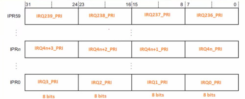
The key thing was to understand the memory layout and that the Number of Priority Bit differs from chip manufacturer and maybe even MCU. For the cortex M4 there are 60 registers with 32 bits.
void GPIO_IRQPriorityConfig(uint8_t IRQNumber, uint8_t IRQPriority)
{
    // There are 60 PR Register and they are sets of 32-bits where each register is 8 bits
    uint8_t ipr_section = IRQNumber / 4;          // Find the section for the 60 PR registers
    uint8_t ipr_section_slot = IRQNumber % 4;     // Find the slot 4 x 8-bit registers

    // The amount of bits depends of the manufacturer
    // For ST the is 4
    uint8_t shift_amount = ( 8 * ipr_section_slot) + (8 - NO_PR_BITS_IMPLEMENTED);

    *(NVIC_PR_BASE_ADDR + ipr_section) |= (IRQPriority  << shift_amount );
}
Set Enable/Clear Register for IRQ (Processor Side)
To enable/disable the IRQ we need to enable the correct NVIC_ISER or NVIC_ICER. In the driver header we set these at the top. These addresses can be found in the Cortex m4.
// Interrupt Set-Enable Register
#define NVIC_ISER0        ( (volatile uint32_t*) 0xE000E100 )
#define NVIC_ISER1        ( (volatile uint32_t*) 0xE000E104 )
#define NVIC_ISER2        ( (volatile uint32_t*) 0xE000E108 )
#define NVIC_ISER3        ( (volatile uint32_t*) 0xE000E10C )

// Interrupt Clear-Enable Register
#define NVIC_ICER0        ( (volatile uint32_t*) 0xE000E180 )
#define NVIC_ICER1        ( (volatile uint32_t*) 0xE000E184 )
#define NVIC_ICER2        ( (volatile uint32_t*) 0xE000E188 )
#define NVIC_ICER3        ( (volatile uint32_t*) 0xE000E18C )
We can create a function in the GPIO driver to set and clear based on IRQ in the driver.
void GPIO_IRQInterruptConfig(uint8_t IRQNumber, uint8_t EnableOrDisable)
{
    // Not % used to find bit position give IRQ is 0-95
    // Position 34 is 34 / 32 gives remainder 2 i.e. position 2
    if (EnableOrDisable == ENABLE)
    {
        if (IRQNumber < 32)
        {
            *NVIC_ISER0 |= (uint32_t)(1 << IRQNumber);
        }
        else if (IRQNumber > 31 && IRQNumber < 64)
        {
            // Program ISER1
            *NVIC_ISER1 |= (1 << IRQNumber % 32);
        }
        else if (IRQNumber > 63 && IRQNumber < 96)
        {
            // Program ISER2
            *NVIC_ISER2 |= (1 << IRQNumber % 64);
        }
    }
    else
    {
        if(IRQNumber < 32) {
            // Program ICER0
            *NVIC_ICER0 |= (1 << IRQNumber);
        } else if(IRQNumber > 31 && IRQNumber < 64) {
            // Program ICER1
            *NVIC_ICER1 |= (1 << IRQNumber  % 32);
        } else if(IRQNumber > 63 && IRQNumber < 96) {
            // Program ICER2
            *NVIC_ICER2 |= (1 << IRQNumber % 64);
        }
    }
}
Clear EXTI PR Register for GPIO Pin (Peripheral Side)
When we want to implement an IRQ handler we need to clear the EXIT PR register by writing 1 for that GPIO pin
void GPIO_IRQHandling(uint8_t PinNumber)
{
    // If the Register is set to 1 for this bit
    //    We clear it  by writing 1
    //    This confused by but presumably this is event driven
    if(EXTI->PR & ( 1 << PinNumber)) {

        // Clear
        EXTI->PR |= (1 << PinNumber );

    }
}
Implement Override IRQ Handler (Application)
Implementing the handler is the easiest part. Default handlers are provided in the .s file provided with the board and run at startup. In the startup code in the .s you will see
.w EXTI0_IRQHandler
.tumb_set EXTI0_IRQHandler, Default_Handler
To override this we need to create a function of the same name in the main. The handler takes no arguments or returns any arguments. We pass the GPIO Pin number to our driver code from above.
// Overriden from .s file
void EXTI0_IRQHandler(void) {
    GPIO_IRQHandling(0);
}
SPI
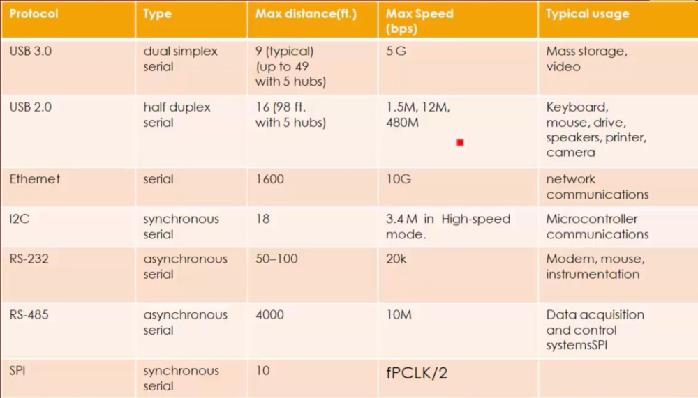
Next we are looking at SPI. Below is a list of possible protocols and usage for MCUs
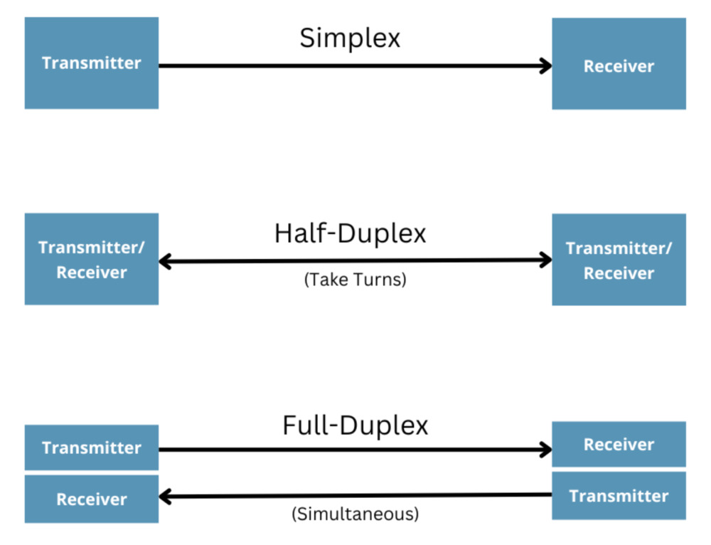
There are 3 SPI modes. These are shown below. Some SPI devices might not support all.
NSS Slave Select Management
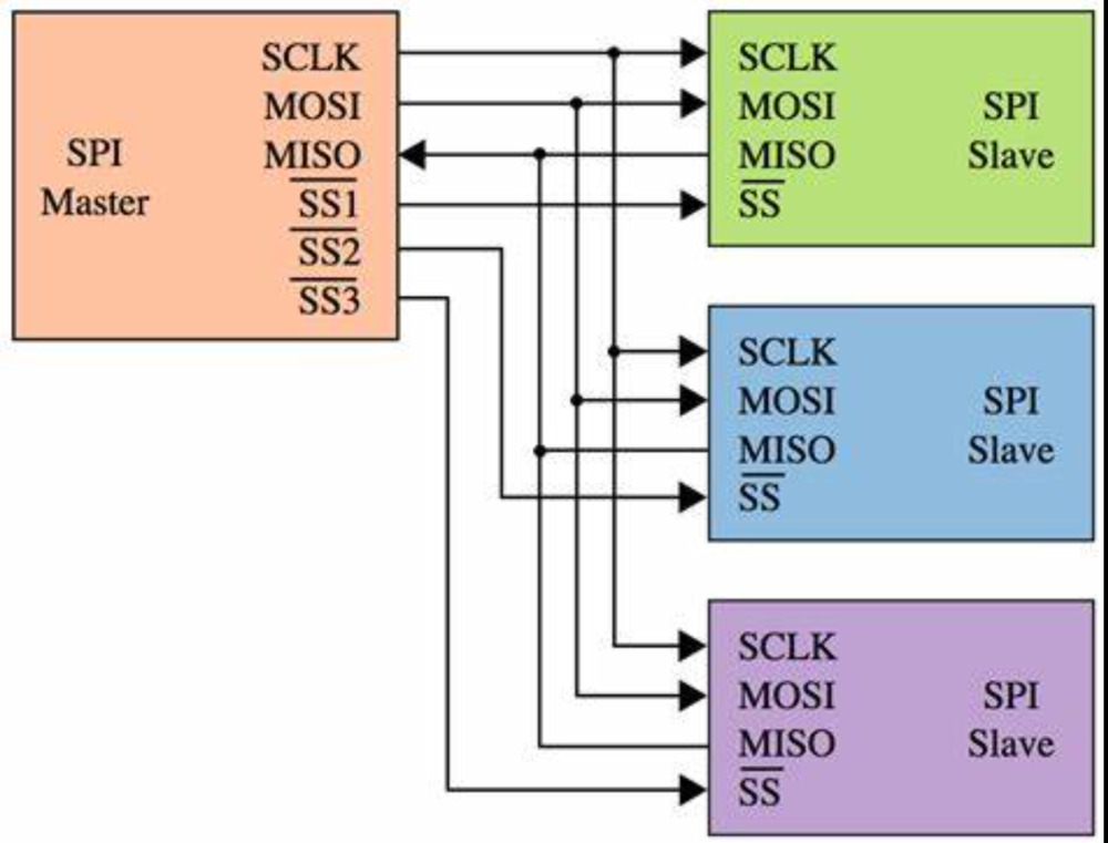
On the slave we can manage the NSS pin for SPI using the SPIx_CR1 register for STM32. This allow us, when SSM=1, to ground the state via the SSI value, SSI=0 is grounded, SSI=1 is pulled high. This frees up the NSS pin for other usage. Otherwise we need to ground this pin.
Where there are multiple slaves you would not use the NSS pin and this would be tied to vdd (high). Separate pins would be used instead for each slave so they can be used independantly.
Communication format
We need to be aware of
- SCLK Phase (CPHA)
- SCLK Polarity (CPOL)
- Data Frame Format (DFF)
Clearly we need both ends to be using the same approach. For the Data Frame Format this is 8-bit or 16-bit depending on MCU. Here is a view of the CLK Phase and Polarity if unconvinced they must be the same.
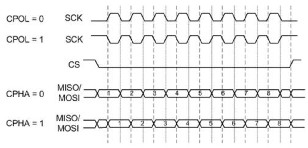
You will need to check the documentation of which mode CPHA/CPOL and device can be configured to.
Clocks
For STM32 there is a HCLK which is the hardware clock. There is a prescaler which divides the clock between the HCLK and the bus.
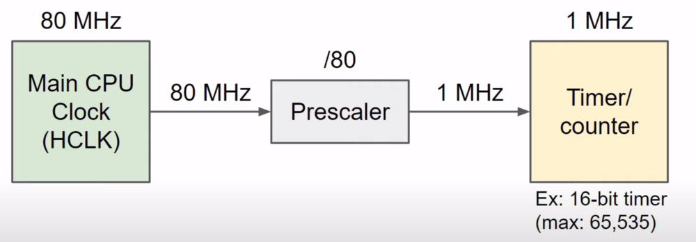
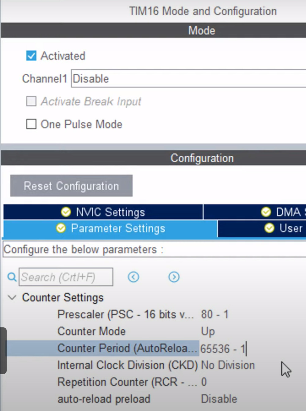
Looking in the clock tree to the reference manual will provide more detail. The Prescalers can be configured to set the desired clockspeed. There is lot of configuration in the STM32 software you can do automatically for timers.
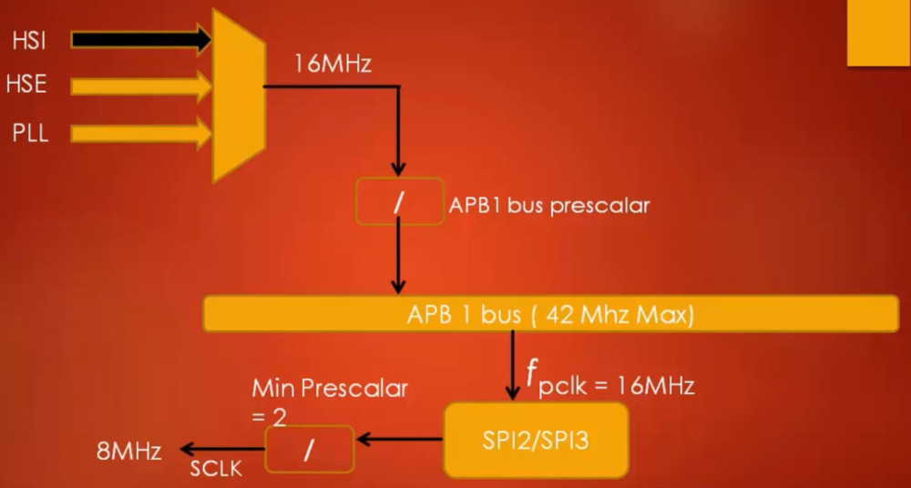
Here is an example of the SPI clock for the course. Because we are using HSI clock the speed is 16Hhz if we used a different clock it could be 42 Mhz. This means the max speed, if using the faster clock could be 21Mhz. In this case we are using 16Hhz so 8Mhz is the speed.
Driver Changes
General
We need to define the register map for SPI using the reference manual
/* SPI Register Map */
typedef struct {

    volatile uint32_t CR1;
    volatile uint32_t CR2;
    volatile uint32_t SR;
    volatile uint32_t DR;
    volatile uint32_t CRCPR;
    volatile uint32_t RXCRCR;
    volatile uint32_t TXCRCR;
    volatile uint32_t I2SCFGR;
    volatile uint32_t I2SPR;

} SPI_RegDef_t;
And macros to access the peripherals
#define SPI1              ((SPI_RegDef_t*)(SPI1_BASEADDR))
#define SPI2              ((SPI_RegDef_t*)(SPI2_BASEADDR))
#define SPI3              ((SPI_RegDef_t*)(SPI3_BASEADDR))
Next we need to define the configuration structure discussed above in a new header for the SPI devices. s
#ifndef __STM32F302_SPI_H__
#define __STM32F302_SPI_H__

#include <stdint.h>
#include "../include/stm32F302xx.h"

/*
 * Configuration Structure to the SPI
 */
typedef struct
{
    uint8_t SPI_DeviceMode;
    uint8_t SPI_BusConfig;
    uint8_t SPI_SclKSpeed;
    uint8_t SPI_DFF;
    uint8_t SPI_CPOL;
    uint8_t SPI_CPHA;
    uint8_t SPI_SSM;

} SPI_Config_t;

/*
 * Handle Structure for a SPI Pin
 */
typedef struct {
    SPI_RegDef_t *pSPIx;
    SPI_PinConfig_t SPI_PinConfig;

} SPI_Handle_t;

#endif
APIs
We can use some of the definitions from the GPIO APIs but we do need to define the send and receive functions
/* Peripheral Clock */
void SPI_PeriClockControl(SPI_RegDef_t *pSPIx, uint8_t EnableOrDisable);

/* Init */
void SPI_Init(SPI_Handle_t *pSPIHandle);
void SPI_DeInit(SPI_RegDef_t *pSPIx);

/* Data Send and Receive */
void SPI_SendData(SPI_RegDef_t *pSPIx, uint8_t *pTxBuffer, uint32_t Len);
void SPI_ReceiveData(SPI_RegDef_t *pSPIx, uint8_t *pRxBuffer, uint32_t Len);

/* IRQ Configuration and ISR Handling */
void SPI_IRQInterruptConfig(uint8_t IRQNumber, uint8_t EnableOrDisable);
void SPI_IRQPriorityConfig(uint8_t IRQNumber, uint8_t IRQPriority);
void SPI_IRQHandling(SPI_Handle_t *pSPIHandle);

/* Other Peripheral Control APIs */
From here we then go and define macros for each value you can use in the configuration options. For example and does not include all fields. These can be generated by co-pilot to save bucket loads of time.
/* Device Mode */
#define SPI_DEVICE_MODE_MASTER 1
#define SPI_DEVICE_MODE_SLAVE 0

/* Bus Config */
#define SPI_BUS_CONFIG_FD 1
#define SPI_BUS_CONFIG_HD 2
#define SPI_BUS_CONFIG_SIMPLEX_RXONLY 3
Send Data
Here is the logic around the send data. Hopefully looking back this will make sense on how to handle 8-bit/16-bit etc. Again co-pilot could get an implementation from the web
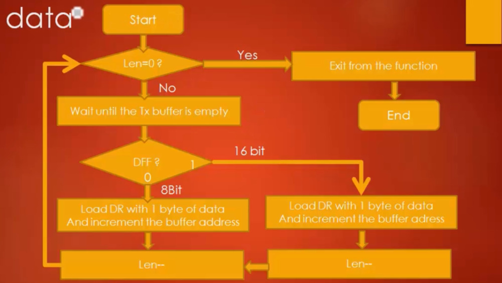
Next we need to write an example to use the function. We can either look at the Reference Manual for Alternative Function mapping or look for pinout diagrams. Took me a while to understand why we should use 5 for SPI but very obvious when you look in the STM32F302r8.pdf manual and the table has AF5
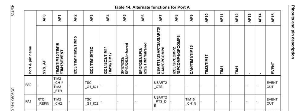
This was quite tricky to get going as had to understand [Type Punning] for the 8-bit part. This is where you copy a pointer of the top of another pointer (I think). My code has improved with sonarlint reminding me to add the volitile. Without it 2 bytes are written for the 8-bit configuration with the Least Significant Byte 0.
void SPI_SendData(SPI_RegDef_t *pSPIx, uint8_t *pTxBuffer, uint32_t Len) {
    while (Len > 0)
    {
        // 1. Wait until TXE is set
        while (SPI_GetFlagStatus(pSPIx, SPI_TXE_FLAG) == FLAG_RESET);

        // 2. Check the DFF bit in CR1
        if ( pSPIx->CR1 & (1 << SPI_CR1_DFF) )
        {
            // 16 bit DFF
            // 1. Load the data into the Data Register
            pSPIx->DR = *((uint16_t *)pTxBuffer);
            Len--;
            Len--;
            pTxBuffer++;
            pTxBuffer++;
        }
        else
        {
            // 8 bit DFF
            // 1. Load the data into the Data Register
            *(volatile uint8_t*)&pSPIx->DR = *pTxBuffer;
            Len--;
            pTxBuffer++;
        }
    }
}
Receive Data
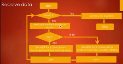
So here is the receive data. It should be getting easier now
Testing
We can use PulseView and a logic analyzer to test this. I had to build the software from scratch on Ubuntu 23.04. Without this then there are no drivers. I did update the udev rules for Saleae so this could be run without root.
SUBSYSTEM=="usb", ENV{DEVTYPE}=="usb_device",  ACTION!="add|change", GOTO="saleae_logic_rules_end"

# Saleae Logic analyzer (USB Based)
# Bus 006 Device 006: ID 0925:3881 Lakeview Research
# Bus 001 Device 009: ID 21a9:1004 Product: Logic S/16, Manufacturer: Saleae LLC

ATTR{idVendor}=="0925", ATTR{idProduct}=="3881", MODE="664", GROUP="plugdev"
ATTR{idVendor}=="21a9", ATTR{idProduct}=="1004", MODE="664", GROUP="plugdev"

LABEL="saleae_logic_rules_end"
I also used the sigrok rules which can be got from their web page