Nano Every Page: Difference between revisions
| Line 6: | Line 6: | ||
Here is the EEPROM. I think I made it look quite pretty with the colours. Funny how that seemed important at the time. | Here is the EEPROM. I think I made it look quite pretty with the colours. Funny how that seemed important at the time. | ||
[[File:EEPROM BEN.jpg]]<br> | [[File:EEPROM BEN.jpg]]<br> | ||
==The Circuit== | |||
I ended up using the circuit from Ben's page. The nano D5 connected to the AT28C256 | |||
==The Code== | ==The Code== | ||
And of course the code. | And of course the code. | ||
| Line 204: | Line 206: | ||
} | } | ||
</syntaxhighlight> | </syntaxhighlight> | ||
==Disabling Software Protection (SDP)== | ==Disabling Software Protection (SDP)== | ||
I did not like the use of PORTC, PORTD etc as this suggested shortcuts and would obfuscate the code. But reading more I found that the code struggled to meet the timings to disable the AT28C256 protections which is why it took me so long to get this going.<br> | I did not like the use of PORTC, PORTD etc as this suggested shortcuts and would obfuscate the code. But reading more I found that the code struggled to meet the timings to disable the AT28C256 protections which is why it took me so long to get this going.<br> | ||
[[File:AT28C256.jpg]]<br> | [[File:AT28C256.jpg]]<br> | ||
Revision as of 03:42, 13 May 2023
Introduction
I while ago I started my interest in the 6502 where it all began to me. This led me to Ben Eater and building an 8-bit computer. Which led me to building a EEPROM programmer and a Nano was required to build it. I had a bit of work to do and my interest seemed to be waning a little. Partly because of the time to get it to work and and because I just felt demotivated. So I solved my motivation by returning to rust and saw that it is possible to run it on a Nano Every. Let the games begin.
Ben's EEPROM
The Board
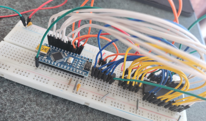
Here is the EEPROM. I think I made it look quite pretty with the colours. Funny how that seemed important at the time.

The Circuit
I ended up using the circuit from Ben's page. The nano D5 connected to the AT28C256
The Code
And of course the code.
#define SHIFT_DATA 2
#define SHIFT_CLK 3
#define SHIFT_LATCH 4
#define WRITE_EN 13

// 32 byte test pattern to verify the EEPROM device.  The pattern includes a walking one
// and a walking zero, which may help to detect pins that are tied together or swapped.
// byte data[] = {
//     'A',  'B',  'C',  'D',  'E',  'F',  'G',  'H',
//     0x01, 0x02, 0x04, 0x08, 0x10, 0x20, 0x40, 0x80,
//     0x7f, 0xbf, 0xdf, 0xef, 0xf7, 0xfb, 0xfd, 0xfe,
//     0x00, 0xff, 0x55, 0xaa, '0',  '1',  '2',  '3'
// };


byte data[] = {
    'A',  'B',  'B',  'D',  'E',  'F',  'G',  'H',
    'A',  'B',  'C',  'D',  'E',  'F',  'G',  'H'
};

void enableWrite()      { digitalWrite(WRITE_EN, LOW);}
void disableWrite()     { digitalWrite(WRITE_EN, HIGH);}


// Read a byte from the data bus.  The caller must set the bus to input_mode
// before calling this or no useful data will be returned.
byte readDataBus() {
    return (PINB << 3) | (PIND >> 5);
}

// Read a byte from the EEPROM at the specified address.
byte readEEPROM(int address) {
    setDataBusMode(INPUT);
    setAddress(address, /*outputEnable*/ true);
    return readDataBus();
}

// Write a byte to the EEPROM at the specified address.
void writeEEPROM(int address, byte data) {
    setAddress(address, /*outputEnable*/ false);
    setDataBusMode(OUTPUT);
    writeDataBus(data);
    enableWrite();
    // delayMicroseconds(1);
    disableWrite();
    delay(10);
}

// Read the first 256 byte block of the EEPROM and dump it to the serial monitor.
void printContents(int size) {
    for (int base = 0; (base < size); base += 16) {
        byte data[16];
        for (int offset = 0; offset <= 15; offset += 1) {
            data[offset] = readEEPROM(base + offset);
        }

        char buf[80];
        sprintf(buf, "%04x:  %02x %02x %02x %02x %02x %02x %02x %02x   %02x %02x %02x %02x %02x %02x %02x %02x",
            base, data[0], data[1], data[2], data[3], data[4], data[5], data[6], data[7],
            data[8], data[9], data[10], data[11], data[12], data[13], data[14], data[15]);
        Serial.println(buf);
    }
}
// Output the address bits and outputEnable signal using shift registers.
void setAddress(int addr, bool outputEnable) {
    // Set the highest bit as the output enable bit (active low)
    if (outputEnable) {
        addr &= ~0x8000;
    } else {
        addr |= 0x8000;
    }
    byte dataMask = 0x04;
    byte clkMask = 0x08;
    byte latchMask = 0x10;

    // Make sure the clock is low to start.
    PORTD &= ~clkMask;

    // Shift 16 bits in, starting with the MSB.
    for (uint16_t ix = 0; (ix < 16); ix++)
    {
        // Set the data bit
        if (addr & 0x8000)
        {
            PORTD |= dataMask;
        }
        else
        {
            PORTD &= ~dataMask;
        }

        // Toggle the clock high then low
        PORTD |= clkMask;
        // delayMicroseconds(3);
        PORTD &= ~clkMask;
        addr <<= 1;
    }

    // Latch the shift register contents into the output register.
    PORTD &= ~latchMask;
    // delayMicroseconds(1);
    PORTD |= latchMask;
    // delayMicroseconds(1);
    PORTD &= ~latchMask;
}

// Write a byte to the data bus.  The caller must set the bus to output_mode
// before calling this or no data will be written.
void writeDataBus(byte data) {
     PORTB = (PORTB & 0xe0) | (data >> 3);
     PORTD = (PORTD & 0x1f) | (data << 5);
}
// Set an address and data value and toggle the write control.  This is used
// to write control sequences, like the software write protect.  This is not a
// complete byte write function because it does not set the chip enable or the
// mode of the data bus.
void setByte(byte value, word address) {
    setAddress(address, false);
    writeDataBus(value);

    // delayMicroseconds(1);
    enableWrite();
    // delayMicroseconds(1);
    disableWrite();
}

// Set the I/O state of the data bus.
// The 8 bits data bus are is on pins D5..D12.
void setDataBusMode(uint8_t mode) {
    // On the Uno and Nano, D5..D12 maps to the upper 3 bits of port D and the
    // lower 5 bits of port B.
    if (mode == OUTPUT) {
        DDRB |= 0x1f;
        DDRD |= 0xe0;
    } else {
        DDRB &= 0xe0;
        DDRD &= 0x1f;
    }
}

void disableSoftwareWriteProtect() {
    disableWrite();
    setDataBusMode(OUTPUT);

    setByte(0xaa, 0x5555);
    setByte(0x55, 0x2aaa);
    setByte(0x80, 0x5555);
    setByte(0xaa, 0x5555);
    setByte(0x55, 0x2aaa);
    setByte(0x20, 0x5555);

    setDataBusMode(INPUT);
    delay(10);
}
void setup() {

  // put your setup code here, to run once:
  pinMode(SHIFT_DATA, OUTPUT);
  pinMode(SHIFT_CLK, OUTPUT);
  pinMode(SHIFT_LATCH, OUTPUT);
  disableWrite();
  pinMode(WRITE_EN, OUTPUT);

  Serial.begin(115200);

  Serial.print("\nDisabling EEPROM Software Data Protection(SDP)...");
  disableSoftwareWriteProtect();
  Serial.println(" done\n");

  // Read and print out the contents of the EERPROM
  Serial.println("Reading EEPROM");
  printContents(32);

  // Program a test pattern and fill the remainder of the first block with 0xff
  Serial.print("Programming EEPROM...");
  for (word address = 0; (address < sizeof(data)); address++) {
      writeEEPROM(address, data[address]);
  }

  // for (word address = sizeof(data); (address < 256); address++) {
  //    writeEEPROM(address, 0xfe);
  // }
  Serial.println(" done\n");

  // Read and print out the contents of the EERPROM
  Serial.println("Reading EEPROM");
  printContents(32);

}

void loop()
{
    // put your main code here, to run repeatedly:
}
Disabling Software Protection (SDP)
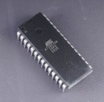
I did not like the use of PORTC, PORTD etc as this suggested shortcuts and would obfuscate the code. But reading more I found that the code struggled to meet the timings to disable the AT28C256 protections which is why it took me so long to get this going.
