Verilog Language: Difference between revisions
| Line 75: | Line 75: | ||
and AND2(out_and2, A, B); | and AND2(out_and2, A, B); | ||
or OR1(Cout, out_and1, out_and2); | or OR1(Cout, out_and1, out_and2); | ||
endmodule | |||
</syntaxhighlight> | |||
On the other page I used boolean logic to implement this. We started with this | |||
S = (A̅.B̅.C ) + (A̅.B.C̅) + (A.B̅.C̅) + (A.B.C) | |||
Cₒᵤₜ = (A̅.B.C ) + (A.B̅.C) + (A.B.C̅) + (A.B.C̅) | |||
And ended with | |||
Cₒᵤₜ = C (A̅ ⊕ B̅) + AB | |||
S = C ⊕ A ⊕ B | |||
<syntaxhighlight lang="v"> | |||
module main( | |||
input A, | |||
input B, | |||
input Cin, | |||
output Cout, | |||
output S | |||
); | |||
// Cout | |||
assign Cout = (Cin & (!A ^ !B) ) | (A & B); | |||
// S | |||
assign S = Cin ^ A ^ B; | |||
endmodule | endmodule | ||
</syntaxhighlight> | </syntaxhighlight> | ||
Revision as of 04:07, 19 December 2024
Introduction
This page is meant to help understand how to approach the language. There are three levels of abstraction.
Way to describe Hardware
- Gate Level
- Dataflow Level
- Behavioral Level
Types of Logic
- Combinational Logic
- Sequential Logic
Combinational Logic
This is where the outputs are a simple function of the inputs. (Sounds like pure functions
2 to 1 Multiplexer using Combinational
This example shows the 3 approaches we can use to describe the hardware
Gate Level
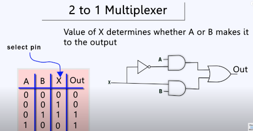
This was quite useful as I have some knowledge of gates and boolean logic so it starts to make a bit of sense in verilog. Here is the truth table for the 2 to 1 multiplexer
To model this at the gate level we could do this
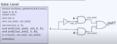
So this is what I learned to get to the answer shown. To solve the problem you name all of the gates, it maybe you name based on type of gate and increment, e.g. and1, and2, and3. These are not shown in the diagram, instead what is named are the wire connecting the gates. These wires need to be declared.
wire not_x;
wire out_and1;
wire out_and2;
- not gate = not1
- and gate (top) = and1
- and gate (bottom) = and2
- or gate = or1
Now to model these we write down the appropriate type, the name, the output, followed by the input so.
- not_x = not not1(not_x, X)
- and1 = and and1(out_and1, A, not_x)
- and2 = and and2(out_and2, X, B)
- out1 = or or1(out1, out_and1, out_and2)
Dataflow Level
And now the Dataflow level. This does look a lot like boolen logic and is very unreadable.

Behavioral Level
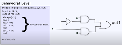
Finally the Behavioral Level which does seem more in my wheel house. The code uses a procedure block where the code only executes when there is a change in the signal
Sequential Logic
Sequential logic uses memory and state. It uses combinational logic too.
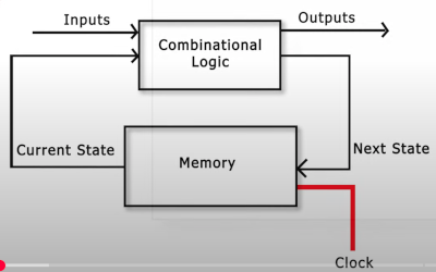
A bit more complex and a bit of memory required on my part.
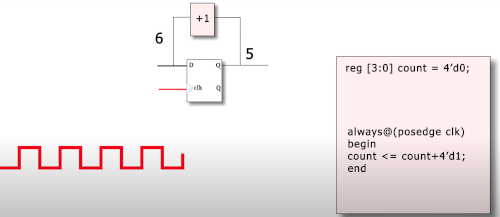
This diagram shows a d-flip flop where the input is the same as the output on a rising edge. The code only executes on a positive edge. It uses a non bloicking assignment <=
Revisiting the Adder
This is when I now understand hopefully how to model gates
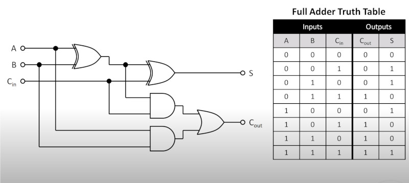
Given this knowledge I
- label the gates
- label the outputs
Which gives this picture
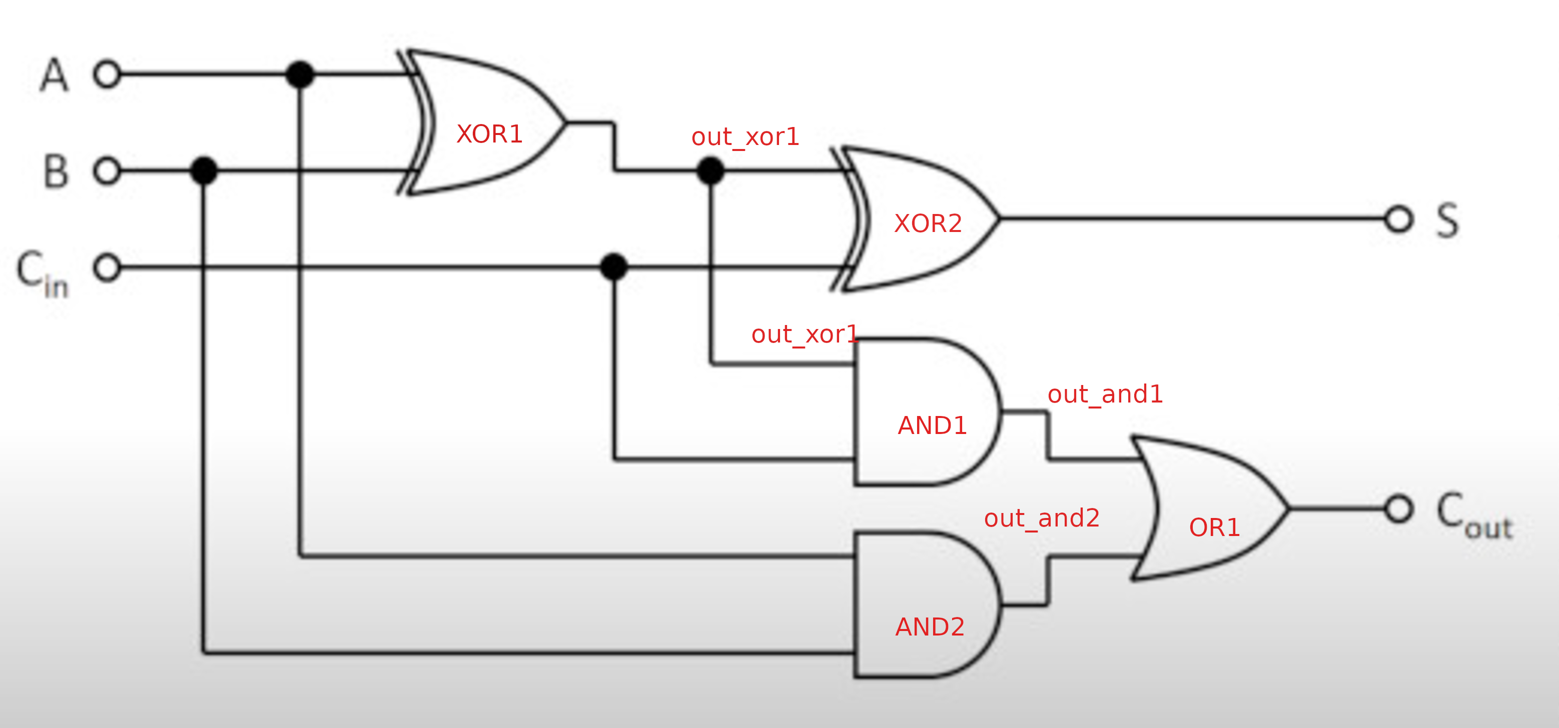
Now we can write the verilog for this using the approach above
module main(
    input A,
    input B,
    input Cin,

    output Cout,
    output S
);
    wire out_xor1;
    wire out_xor2;
    wire out_and1;
    wire out_and2;

    xor XOR1(out_xor1, A, B);
    xor XOR2(S, out_xor1, Cin);
    and AND1(out_and1, out_xor1, Cin);
    and AND2(out_and2, A, B);
    or  OR1(Cout, out_and1, out_and2);
endmodule
On the other page I used boolean logic to implement this. We started with this
S    = (A̅.B̅.C ) +  (A̅.B.C̅) + (A.B̅.C̅) + (A.B.C)
Cₒᵤₜ = (A̅.B.C ) +  (A.B̅.C) + (A.B.C̅) + (A.B.C̅)
And ended with
Cₒᵤₜ = C (A̅ ⊕ B̅) + AB
S    = C ⊕ A ⊕ B
module main(
    input A,
    input B,
    input Cin,

    output Cout,
    output S
);
    // Cout
    assign Cout = (Cin & (!A ^ !B) ) | (A & B);

    // S
    assign S = Cin ^ A ^ B;

endmodule
Language Quick Reference
Here is a quick reference File:Verilog Quick Reference Card v2 0.pdf