STM32 Page
Introduction
This is the page for all things STM32. Currently working with a Nucleo F302R8
Setting Up
This was a trial and a half and here in case some others struggle and find this help.
STM32CubeIDE (Eclipse)
My goal was to use eclipse because this is what is used in the videos. So with ubuntu 23.04 install went to install this with eclipse. But the eclipse version requires python 2.7 which is no longer available.
VS Code
Luckily STM32 had brought out an extensions for my preferred solution VS Code. Installed the extension and went about installing the 3 other products it mentioned.
- STM32CubeMX
- STMCUFinder
- stm32cubeclt_1.12.1
Started it up but the import project button did nothing at all so I assumed it must need STM32CubeIDE. So went back to trying to install libpython2.7 and found https://askubuntu.com/questions/101591/how-do-i-install-the-latest-python-2-7-x-or-3-x-on-ubuntu. Unfortunately whatever I did must have move ld.so or something serious so had to re-install. But the good news was I could retry the STM32 extension. Having a new install I tried the STM32 Extension and it did indeed say could not find STM32CubeIDE. I documented this on the STM32 forum under https://community.st.com/s/question/0D53W00002IMDFZSA5/import-project-in-vs-code-ubuntu-2404
STM32CubeIDE Attempt 2
The was an additional install for STM32CubeIDE for vanilla linux. So I downloaded this and installed it. But on start up it failed with an error org.eclipse.swt.internal.C::strlen.
But the next morning googling I found https://github.com/adoptium/adoptium-support/issues/785 and the solution to getting it to work.
mkdir /tmp/SWT-GDBusServer
So may find solution was
- Ubuntu 23.04
- en.st-stm32cubeide_1.12.1_16088_20230420_1057_amd64.sh.zip
- en.ST-MCU-FinderLin_v5-0-0.zip
- en.stm32cubemx-lin-v6-8-1.zip
Debugging
Getting Started
Well now have all of the bits installed. Next it is time to start debugging
Update nucleo f302r8
This required an Update to the firmware. Google is your friend. Downloaded en.stsw-link007-v3-12-3.zip. This contained the udev rules which you can install using dpkg. Don't forget to reload rules with
sudo udevadm control --reload-rules
sudo udevadm trigger
Next under the stsw-link007/AllPlatforms
sudo java -jar STLinkUpgrade.jar
Hopefully this all goes well
Launch Settings
This was surprisingly easy once I had all the other things in place. Here is my file.
{
  "version": "0.2.0",
  "configurations": [

    {
      "name": "Debug via ST-Link",
      "cwd": "${workspaceRoot}",
      "type": "cortex-debug",
      "executable": "./build/debug/build/Test6.elf",
      "request": "launch",
      "servertype": "stlink",
      "device": "STM32F02R8",
      "interface": "swd",
      "runToEntryPoint": "main",
      "svdFile": "STM32F302.svd",
      "v1": false,
      "showDevDebugOutput": "both",
      "armToolchainPath": "/opt/st/stm32cubeclt_1.12.1/GNU-tools-for-STM32/bin"
  },
  ]
}
I used the following files for help
- Marus on Github https://github.com/Marus/cortex-debug/blob/master/debug_attributes.md
- MaJerle on Github https://github.com/MaJerle/stm32-cube-cmake-vscode/blob/main/README.md
Blinky
Did take me a while to read the documentation. Especially around finding the LEDs on the board. Starting a new app provided the proper view. Maybe it is something I need to learn. Also lost a bit of time putting the code in the main rather than in the while loop further down. So here is the setting of GPIO pins STM32 style.
  /* Infinite loop */
  /* USER CODE BEGIN WHILE */
  while (1)
  {
    /* USER CODE END WHILE */

      // HAL_GPIO_TogglePin(GPIOB, GPIO_PIN_13);
      // HAL_Delay(500);
      if(HAL_GPIO_ReadPin(GPIOC,GPIO_PIN_13) == GPIO_PIN_RESET) {
        HAL_GPIO_WritePin(GPIOB, GPIO_PIN_13, GPIO_PIN_SET);
        HAL_Delay(500);
        HAL_GPIO_WritePin(GPIOB, GPIO_PIN_13, GPIO_PIN_RESET);
      }

    /* USER CODE BEGIN 3 */
  }
  /* USER CODE END 3 */
Memory
Almost forgot to do this. So we now have this working in VS Code. Some brief reminders of some basics with regard to memory. So here is some simple code to copy some data from flash to the SRAM. On the board I have SRAM starts at 0x20000000.
char const myData[]  = "I love Programming";
#define BASE_ADDRESS_OF_SRAM 0x20000000

void foo2() {
  for(int i = 0; i < sizeof(myData); i++) {
    *((uint8_t*) BASE_ADDRESS_OF_SRAM +i ) = myData[i];
  }
}
With eclipse you can add a memory window and set the format to ASCII and then go to the location to see the copy.
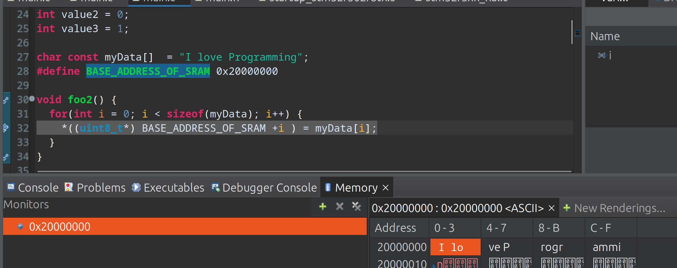
For VS Code I have struggled to get this going with hex 0x20000000 but for decimal 536870912 this works fine.

By adding &myData you can view the address in the memory view too. We can see here that myData is stored at 0x8002864. I have used the fred variable to demonstrate this. You can see the actual address is the first address in the memory view in yellow 0x8002864 however the display in white starts at 0x8002860.

System Architecture
Introduction
My knowledge is very small, no not just in general, but on this subject in computers. This is probably where I regret not having a degree. But here goes I am going to try and understand enough of the diagram from the STM32F0xx Cortex-M0 to be dangerous.
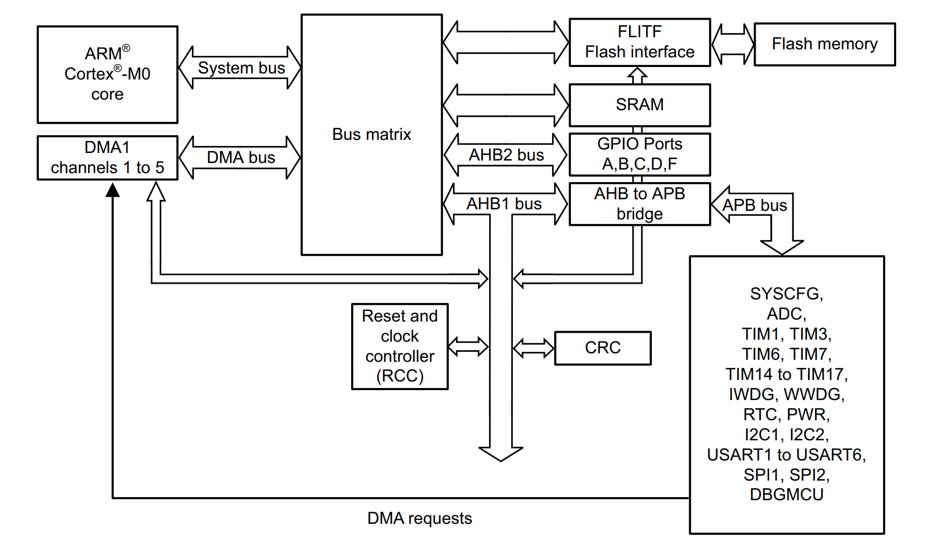
I am again looking at Intermation and their course which is Computer Organization and design.
NVIC and EXTI
Not fully on board with this but the NVIC (Nested Vectored Interrupt Controller) is a interrupt controller connected to the CPU. From one of the docs (STM32G4) it lists its features as
- 102 interrupt sources,
- 16 programmable priority levels,
- Low-latency exception and interrupt handling,
- Automatic nesting,
- Power management control.
In the lesson I was doing this came up because of the EXTI (EXTernal Interrupt/Event) controller which is connected to the NVIC. When using CubeMX you can configure handlers for the GPIO pin which connects to the EXTI on the NVIC. In my case there are 28 lines on the EXTI
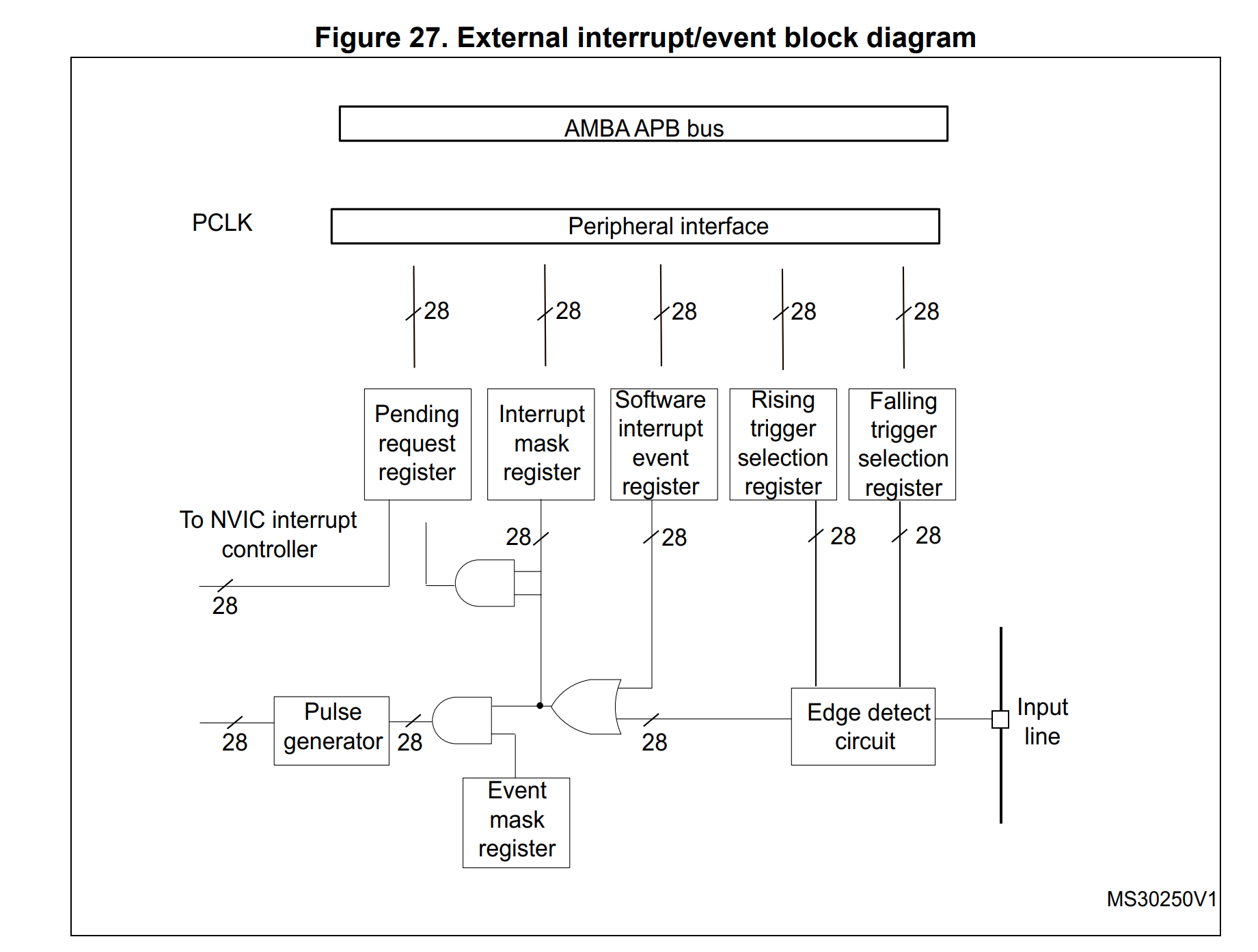
Pending Request Register
When we press a button it is flagged in the pending request register shown above. We can get the address of the register from the manual. In the case of the STM32F302R8 we can first find the EXTI in the manual
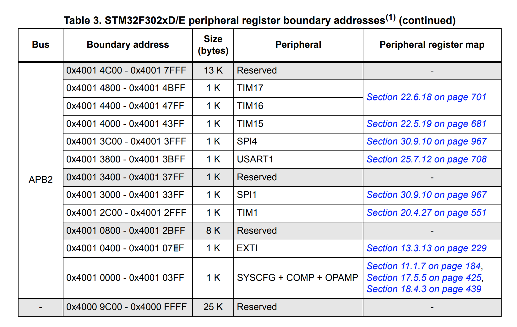
This is probably more about navigating the documentation than the detail but here is the EXTI_PR1 document. After all the software is easy
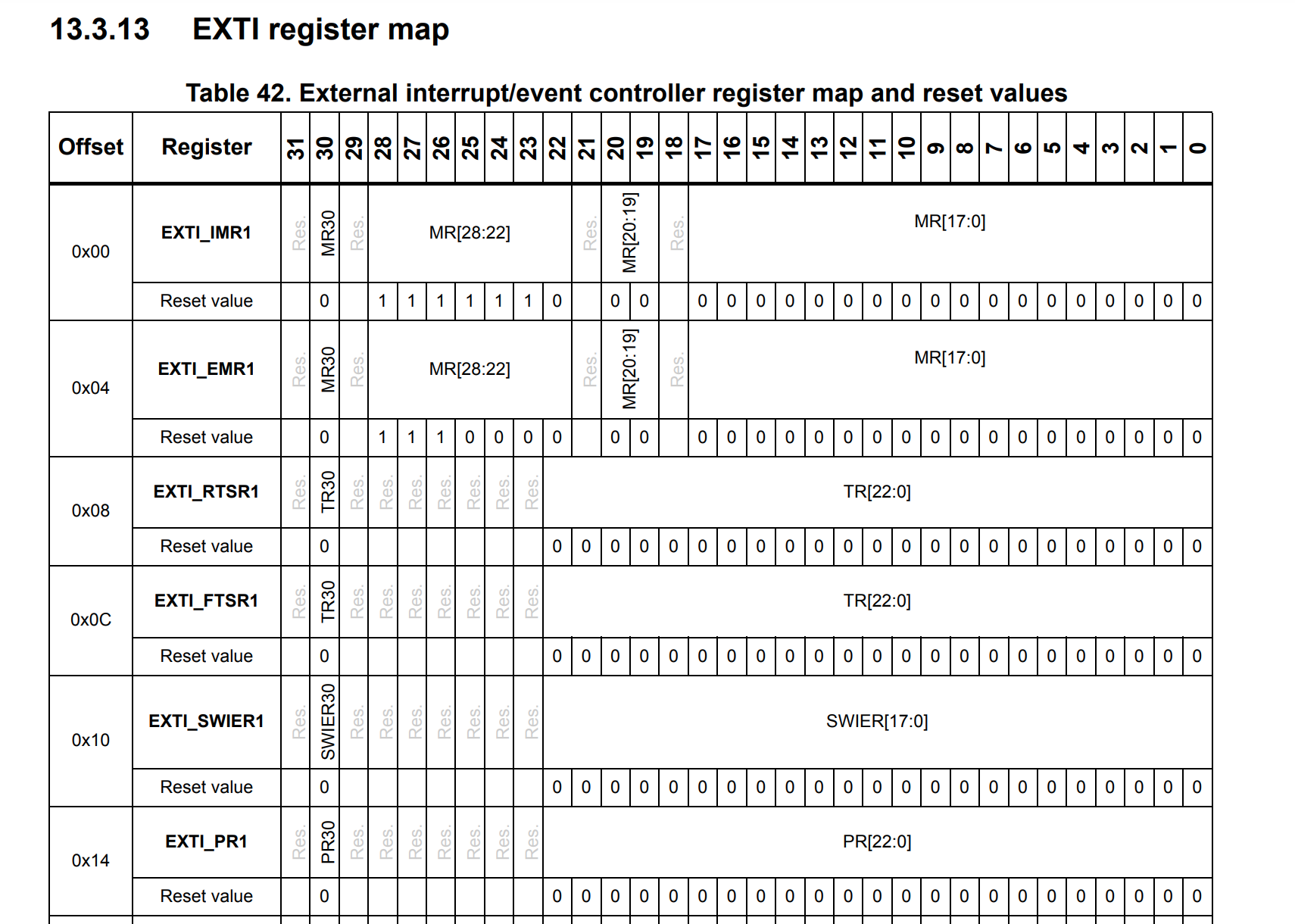
So the address of the EXIT is 0x4001 0400 - 0x4001 07FF and when we look for EXTI_PR1 it is offset 0x14 so the address is 0x4001 0414.
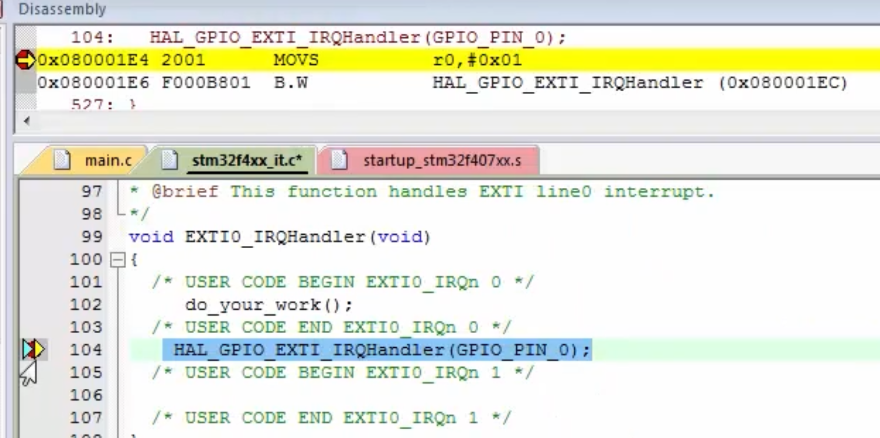
They were very keen to stress that it is the programmers (so old fashioned) job to clear the bit in the PR when done. Using the CubeMX this is what is generated for you via macros.
STM32 Header Files
Briefly ARM have a thing called CMIS. Vendors follow these guidelines and share common macros etc.
Volatile Keyword
Looking at the headers at lot of the headers specify volatile. This forces the compiler to always read the value and not optimize out. With an optimizer the value of p in the code below is not updated and remains in the first loop if the volatile keyword is not used.
#include <stdint.h>


#define SRAM_ADDRESS1   0x20000004U

int main(void)
{

  uint32_t value = 0;
  uint32_t volatile *p = (uint32_t *) SRAM_ADDRESS1;

    while(1)
  {
   value = *p;
   if(value) break;

  }

  while(1);

  return 0;
}
GPIO and Ports
Resetting Ports
Again for documentation most of the STM32 boards will list the peripheral and have the register as the last entry. When you look at the ports some of the reset value might not be neccessarily 0x000 0000. For the STM32F302R8 they were
Address offset:0x00
- Reset value: 0xA800 0000 for port A
- Reset value: 0x0000 0280 for port B
- Reset value: 0x0000 0000 for other ports
Each GPIO should have a pullup resistor. This ensures pins are not floating,neither positive or negative, which will happen due to residual voltage. The pullup resistor value can be found in the documentation searching for Rₚᵤ. or Weak Pull-up.
GPIO Modes
A bit was said about this and the importance of using pullup resistors. The open drain setting was brought up with I2C so may come back to this.
- Input
- Output
- Push/Pull (0 or 1)
- Open Drain (0 or floating)
Speed (Output Only)
We can set the speed of the output using the OSPEEDRy. There are two bits for each port this effect the rising time and falling time. You have to refer to the datasheet (separate from reference manual) to understand the different available speeds. Search for OSPEEDS. I will be very happy if I ever need this. The speed are based on the voltage and clock capacitance.
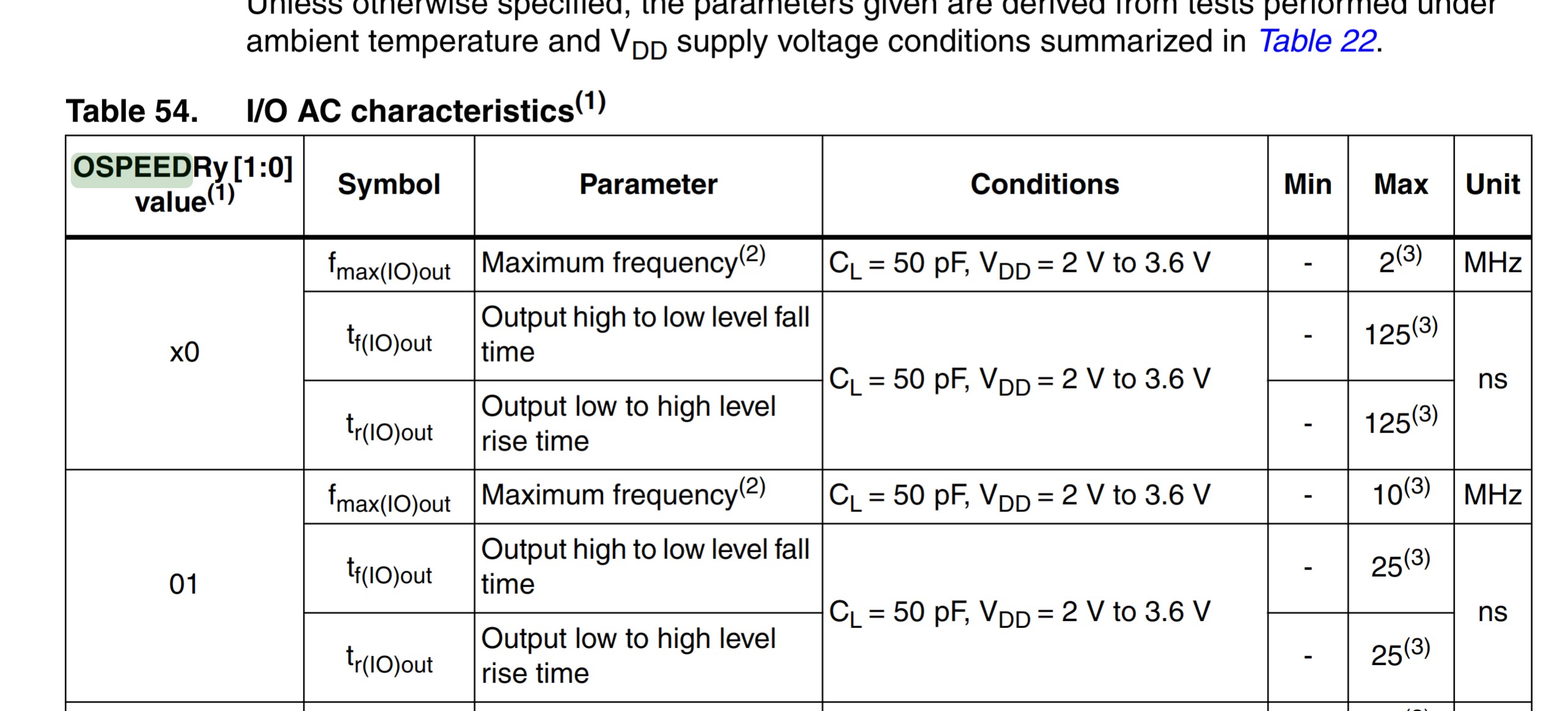
A use case I have heard for setting these speeds is bit-banging which currently I do not understand but believe you could fake an interface by this technique.
The slew rate is defined as the maximum rate of output voltage change per unit time. It is denoted by the letter S. The slew rate helps us to identify the amplitude and maximum input frequency suitable to an operational amplifier (OP amp) such that the output is not significantly distorted.
Alternate Function Mapping
There are 16 different alternate functions pins can be used for. For STM you can generally see this on the pinout when googling but he datasheet also holds a table Alternate Function Mapping showing which pins support what. These can be configured using the Alternate Function Register High (AFRH) and Alternate Function Register Low (AFRL)
STM32 Driver Creation
Introduction
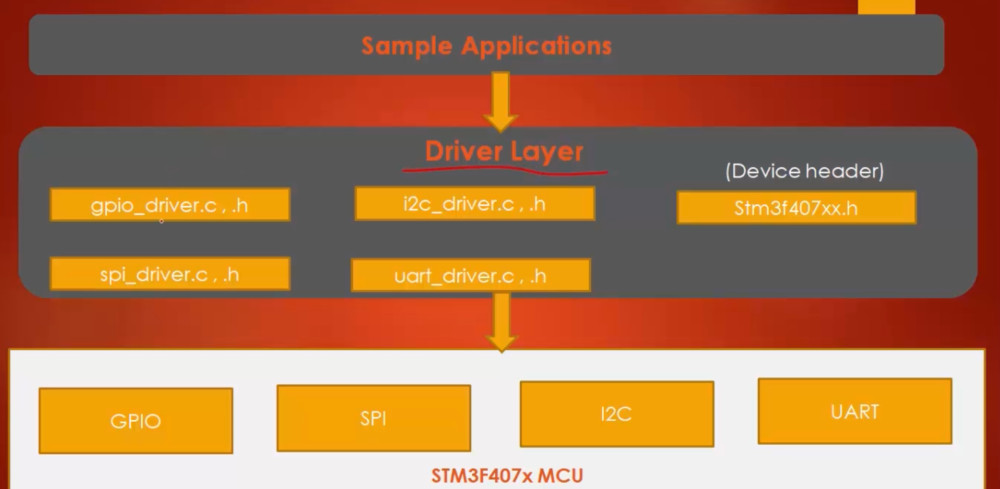
This is the start of creating a driver. This is the introd slide where they explained the next few steps.
Creating a Device Specific Driver File
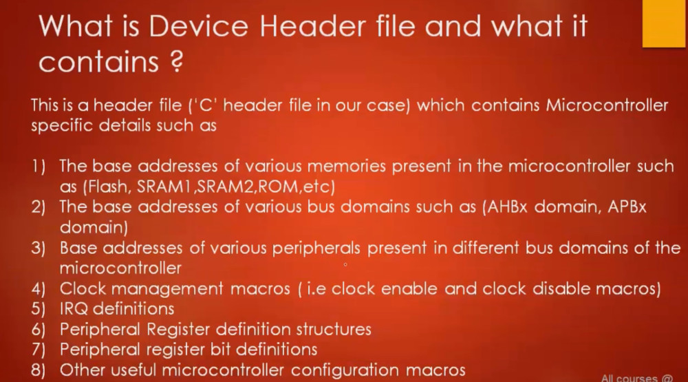
This is creating a header file which will contain the necessary headers for the peripherals and used in the Application. They suggested this should contain.
Memory Addresses
Created a header adding addresses from the controller
#ifndef __stm32F302__h
#define __stm32F302__h

/*
 * Base address of Flash and RAM
 * Note we can either cast to (uint32_t) or add a U to denote
 * unsigned to the compiler
 * SROM is labelled System Memory in the Reference Manual
 */

#define FLASH_BASEADDR  0x08000000U
#define SRAM1_BASEADDR  0x20000000U
#define SRAM            SRAM1_BASEADDR
#define ROM_BASEADDR    0x1FFFD800U
#endif
Bus Domains
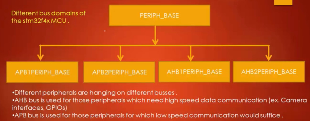
Next we move on the the Bus domains
...
/*
 * AHBx and APBx Bus Peripheral Base Address
 * These were list in reverse order in the
 * Reference manual
 */

#define AHB3PERIPH_BASE 0x50000000U
#define AHB2PERIPH_BASE 0x48000000U
#define AHB1PERIPH_BASE 0x40020000U
#define APB2PERIPH_BASE 0x40010000U
#define APB1PERIPH_BASE 0x40000000U
Peripherals
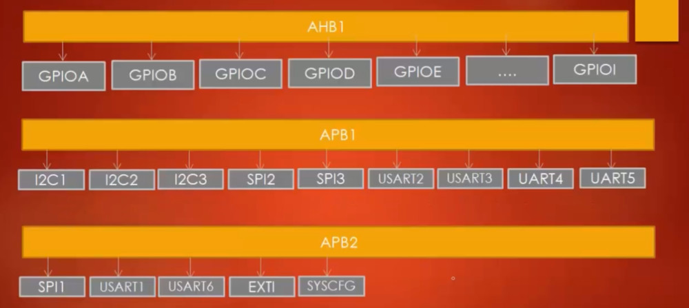
And now the actual peripherals
...
/*
 * Base address of all hanging off AHB1
 */
#define RCC_BASEADDR    (AHB1PERIPH_BASE + 0x1000)

/*
 * Base address of all hanging off AHB2
 */
#define GPIOA_BASEADDR  (AHB2PERIPH_BASE + 0x0000)
#define GPIOB_BASEADDR  (AHB2PERIPH_BASE + 0x0400)
#define GPIOC_BASEADDR  (AHB2PERIPH_BASE + 0x0800)
#define GPIOD_BASEADDR  (AHB2PERIPH_BASE + 0x0C00)
#define GPIOE_BASEADDR  (AHB2PERIPH_BASE + 0x1000)
#define GPIOF_BASEADDR  (AHB2PERIPH_BASE + 0x1400)

/*
 * Base address of all hanging off APB1
 */
#define SPI2_BASEADDR    (APB1PERIPH_BASE + 0x3800)
#define SPI3_BASEADDR    (APB1PERIPH_BASE + 0x3C00)
#define USART2_BASEADDR  (APB1PERIPH_BASE + 0x4400)
#define USART3_BASEADDR  (APB1PERIPH_BASE + 0x4800)
#define UART4_BASEADDR   (APB1PERIPH_BASE + 0x4C00)
#define UART5_BASEADDR   (APB1PERIPH_BASE + 0x5000)
#define I2C1_BASEADDR    (APB1PERIPH_BASE + 0x5400)
#define I2C2_BASEADDR    (APB1PERIPH_BASE + 0x5800)

/*
 * Base address of all hanging off APB2
 */
#define SYSCFG_BASEADDR    (APB2PERIPH_BASE + 0x0000)
#define EXTI_BASEADDR      (APB2PERIPH_BASE + 0x0400)
#define SPI1_BASEADDR      (APB2PERIPH_BASE + 0x3000)
#define USART1_BASEADDR    (APB2PERIPH_BASE + 0x3800)
Note the USARTx and UARTx. UARTx do not support synchronous communication. They cannot use the serial (output) clock.
Registers
Next the Registers
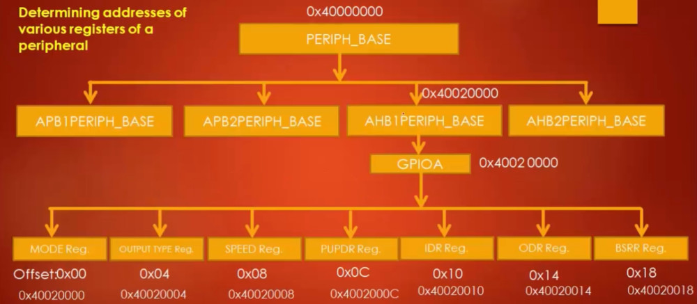
We look in the Reference Manual under GPIO register map and we map their structure in a C struct.
...
/* GPIO Register Map */
typedef struct {

    volatile uint32_t MODER;
    volatile uint32_t OTYPER;
    volatile uint32_t OSPEEDR;
    volatile uint32_t PUPDR;
    volatile uint32_t IDR;
    volatile uint32_t ODR;
    volatile uint32_t BSRR;
    volatile uint32_t LCKR;
    volatile uint32_t AFR[2];

} GPIO_RegDef_t;
Now the RCC Register
...
/* RCC Register Map */
typedef struct {

    volatile uint32_t CR;
    volatile uint32_t CFGR;
    volatile uint32_t CIR;
    volatile uint32_t APB2RSTR;
    volatile uint32_t APB1RSTR;
    volatile uint32_t APB2ENR;
    volatile uint32_t APB1ENR;
    volatile uint32_t BDCR;
    volatile uint32_t CSR;
    volatile uint32_t AHBRSTR;
    volatile uint32_t CFGR2;
    volatile uint32_t CFGR3;

} RCC_RegDef_t;
...
And now the peripherals
/* Peripheral Addresses */
#define GPIOA             ((GPIO_RegDef_t*)(GPIOA_BASEADDR))
#define GPIOB             ((GPIO_RegDef_t*)(GPIOB_BASEADDR))
#define GPIOC             ((GPIO_RegDef_t*)(GPIOC_BASEADDR))
#define GPIOD             ((GPIO_RegDef_t*)(GPIOD_BASEADDR))
#define GPIOE             ((GPIO_RegDef_t*)(GPIOE_BASEADDR))
#define GPIOF             ((GPIO_RegDef_t*)(GPIOF_BASEADDR))

#define RCC               ((RCC_RegDef_t*)(RCC_BASEADDR))
#define EXI               ((RCC_RegDef_t*)(EXTI_BASEADDR))
...
Macros Enable/Disable
Enable
To enable a bit we use the or operator and shift 1 into the specified bit position
( address |= ( value << position )
For example to set a 1 in RCC->APB2ENR bit 12
#define ENABLE_THIS (RCC->APB2ENR |= (1 << 12))
Disable
To disable a bit we use the and operator and negated shift 1 into the specified bit position
( address &= ~( value << position )
For example to set a 0 in RCC->APB2ENR bit 12
#define DISABLE_THIS (RCC->APB2ENR &= ~(1 << 12))
And here are the macros for the peripherals above
...
/* Clock Enable Macros for GPIOx peripherals */
#define GPIOA_PCLK_EN() (RCC->AHBENR |= (1 << 17))
#define GPIOB_PCLK_EN() (RCC->AHBENR |= (1 << 18))
#define GPIOC_PCLK_EN() (RCC->AHBENR |= (1 << 19))
#define GPIOD_PCLK_EN() (RCC->AHBENR |= (1 << 20))
#define GPIOE_PCLK_EN() (RCC->AHBENR |= (1 << 21))
#define GPIOF_PCLK_EN() (RCC->AHBENR |= (1 << 22))

/* Clock Enable Macros for I2Cx peripherals */
#define I2C1_PCLK_EN() (RCC->APB1ENR |= (1 << 21))
#define I2C2_PCLK_EN() (RCC->APB1ENR |= (1 << 22))

/* Clock Enable Macros for SPIx peripherals */
#define SPI2_PCLK_EN() (RCC->APB1ENR |= (1 << 14))
#define SPI3_PCLK_EN() (RCC->APB1ENR |= (1 << 15))
#define SPI1_PCLK_EN() (RCC->APB2ENR |= (1 << 12))

/* Clock Enable Macros for USARTx peripherals */
#define USART1_PCLK_EN() (RCC->AHB2ENR |= (1 << 14))
#define USART2_PCLK_EN() (RCC->AHB1ENR |= (1 << 17))
#define USART3_PCLK_EN() (RCC->AHB1ENR |= (1 << 18))

/* Clock Enable Macros for SYSCFG peripherals */
#define SYSCFG_PCLK_EN() (RCC->AHB1ENR |= (1 << 0))


/* Clock Disable Macros for GPIOx peripherals */
#define GPIOA_PCLK_DI() (RCC->AHB1ENR &= ~(1 << 17))
#define GPIOB_PCLK_DI() (RCC->AHB1ENR &= ~(1 << 18))
#define GPIOC_PCLK_DI() (RCC->AHB1ENR &= ~(1 << 19))
#define GPIOD_PCLK_DI() (RCC->AHB1ENR &= ~(1 << 20))
#define GPIOE_PCLK_DI() (RCC->AHB1ENR &= ~(1 << 21))
#define GPIOF_PCLK_DI() (RCC->AHB1ENR &= ~(1 << 22))

/* Clock Disable Macros for I2Cx peripherals */
#define I2C1_PCLK_DI() (RCC->APB1ENR &= ~(1 << 21))
#define I2C2_PCLK_DI() (RCC->APB1ENR &= ~(1 << 22))


/* Clock Disable Macros for SPIx peripherals */
#define SPI1_PCLK_DI() (RCC->APB2ENR &= ~(1 << 12))
#define SPI2_PCLK_DI() (RCC->APB1ENR &= ~(1 << 14))
#define SPI3_PCLK_DI() (RCC->APB1ENR &= ~(1 << 15))


/* Clock Disable Macros for USARTx peripherals */
#define USART1_PCLK_DI() (RCC->AHB2ENR &= ~(1 << 14))
#define USART2_PCLK_DI() (RCC->AHB1ENR &= ~(1 << 17))
#define USART3_PCLK_DI() (RCC->AHB1ENR &= ~(1 << 18))

/* Clock Disable Macros for SYSCFG peripherals */
#define SYSCFG_PCLK_DI() (RCC->AHB1ENR &= ~(1 << 0))
GPIO Driver File
Next we create a file defining the API for GPIO we will support and structures to support it
There was lots of functions but main it was about reading, setting and clearing bits.
- Setting a bit
Use the bitwise OR operator (|) to set a bit.
number |= 1 << x;
That will set a bit x.
- Clearing a bit
Use the bitwise AND operator (&) to clear a bit.
number &= ~(1 << x);
That will clear bit x. You must invert the bit string with the bitwise NOT operator (~), then AND it.
- Toggling a bit
The XOR operator (^) can be used to toggle a bit.
number ^= 1 << x;
Blinky on Steriods
Introductions
This was a journey to build a blinky for STM32 using this new knowledge of how to build a HAL. Luckily there is always out there. Many thanks for AFontaine79. Lots of experience with this but near to none on arm so the example https://github.com/AFontaine79/stm-blinky put me on by way.
Detail
Really this is to provide the framework for making an ARM binary. I include the STM32 propriety software and the ARM headers to make this all work. So I need the CMSIS directory which comes with CubeMX and the cortex headers which come with the ARM SDK. In the end the project looked like this, where HAL is where my own hal files are.
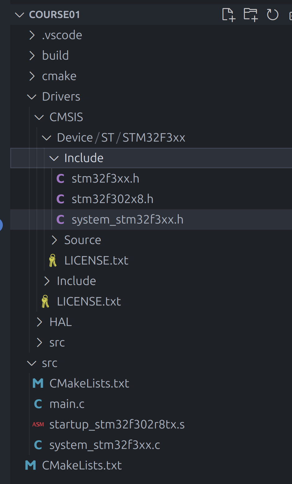
An where is my blinky
#include "stm32F302xx.h"
#include "stm32F302_gpio.h"

void delay(void) {
    for(uint32_t i=0; i<5000/2;i++);
}

int main(void) {
    GPIO_Handle_t GpioLed;

    GpioLed.pGPIOx = GPIOB;
    GpioLed.GPIO_PinConfig.GPIO_PinNumber = GPIO_PIN_NO_13;
    GpioLed.GPIO_PinConfig.GPIO_PinMode = GPIO_MODE_OUTPUT;
    GpioLed.GPIO_PinConfig.GPIO_PinSpeed = GPIO_SPEED_LOW;
    GpioLed.GPIO_PinConfig.GPIO_PinOPType = GPIO_OP_TYPE_PP;
    GpioLed.GPIO_PinConfig.GPIO_PinPuPdControl = GPIO_PIN_NO_PUPD;

    GPIO_PeriClockControl(GPIOB, ENABLE);

    GPIO_Init(&GpioLed);

    while (1) {
        // GPIO_WriteToOutputPin(GPIOB, GPIO_PIN_NO_13, GPIO_PIN_SET);
        GPIO_ToggleOutputPin(GPIOB, GPIO_PIN_NO_13);
        delay();
        //GPIO_WriteToOutputPin(GPIOB, GPIO_PIN_NO_13, GPIO_PIN_RESET);
    }
    {
        /* code */
    }

    return 0;
}
IRQs
Introduction
The is how to handle IRQs for the STM32 devices. So far we have slide which I need to add more comments.
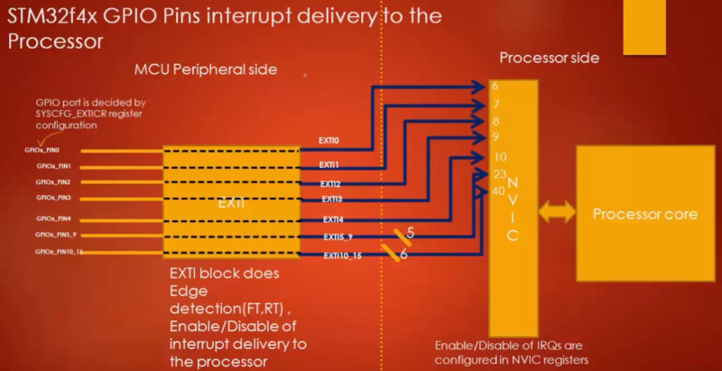
- IRQs disabled by default
- Set the GPIO port to use
- Lines 5-9 are connected to 23
- Lines 10-15 are connected to 40
- Vector table hold information 23 and 40
At the time they mentioned the Peripheral side vs Processor side. What they meant was the non-chip side. I.E. the part provided by STM32 and the part provided by ARM Cortex m4
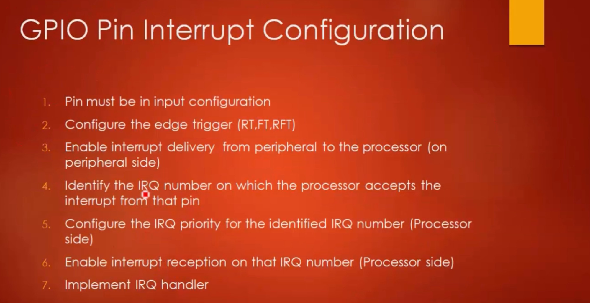
Actual Steps
The video seem to make its own names for dithered on what the steps are. I am going to do the same using my own point of view
- Configure The Edge Trigger RT, FT and RFT (Peripheral Side)
- Enable Delivery from the Peripheral to the Processor (Peripheral Side)
- Identify the EXTI Line based on the GPIO Pin Number (Peripheral Side)
- Configure Priority (Processor Side)
- Set Enable/Clear Register for IRQ (Processor Side)
- Clear EXTI PR Register for GPIO Pin (Peripheral Side)
- Implement Override IRQ Handler (Application)
Configure GPIO Pin
Here are the steps to configuring the GPIO Pins based on the video
Configure The Edge Trigger RT, FT and RFT (Peripheral Side)
So we need to create the structures similar to RCC to hold EXTI and SYSCFG in the driver
/* EXI Register Map */
typedef struct {
    volatile uint32_t IMR;
    volatile uint32_t EMR;
    volatile uint32_t RTSR;
    volatile uint32_t FTSR;
    volatile uint32_t SWIER;
    volatile uint32_t PR;
    volatile uint32_t RESERVED1;
    volatile uint32_t RESERVED2;
    volatile uint32_t IMR2;
    volatile uint32_t EMR2;
    volatile uint32_t RTSR2;
    volatile uint32_t FTSR2;
    volatile uint32_t SWIER2;
    volatile uint32_t PR2;
} EXTI_RegDef_t;

/* SYSCFG Register Map */
typedef struct {
    volatile uint32_t CFGR1;
    volatile uint32_t EXTICR[4];
    volatile uint32_t CFGR2;
} SYSCFG_RegDef_t;
Now in the GPIO_Init function we configure the edge trigger. When setting one trigger we clear the other to ensure consistency.
void GPIO_Init(GPIO_Handle_t *pGPIOHandle) {
...
        if (pGPIOHandle->GPIO_PinConfig.GPIO_PinMode == GPIO_MODE_IT_FT)
        {
            // 1. Configure FTSR
            // Set bit for FTSR
            EXTI->FTSR |= (1 << pGPIOHandle->GPIO_PinConfig.GPIO_PinNumber);
            // Clear bit for RTSR
            EXTI->RTSR &= ~(1 << pGPIOHandle->GPIO_PinConfig.GPIO_PinNumber);
        }

        else if (pGPIOHandle->GPIO_PinConfig.GPIO_PinMode == GPIO_MODE_IT_RT)
        {

            // Set bit for RTSR
            EXTI->RTSR |= (1 << pGPIOHandle->GPIO_PinConfig.GPIO_PinNumber);
            // Clear bit for FTSR
            EXTI->FTSR &= ~(1 << pGPIOHandle->GPIO_PinConfig.GPIO_PinNumber);
        }
        else if (pGPIOHandle->GPIO_PinConfig.GPIO_PinMode == GPIO_MODE_IT_RFT)
        {

            // 1. Configure FTSR and RFSR
            EXTI->FTSR |= (1 << pGPIOHandle->GPIO_PinConfig.GPIO_PinNumber);
            EXTI->RTSR |= (1 << pGPIOHandle->GPIO_PinConfig.GPIO_PinNumber);
        }
...
Enable Delivery from the Peripheral to the Processor (Peripheral Side)
Carrying on in GPIO_Init we set the Port in the EXICR (EXTI Configuration Register). For our device the are four of these.
void GPIO_Init(GPIO_Handle_t *pGPIOHandle) {
...
        // 2. Configure the GPIO port selection in SYSCFG_EXICR
        uint8_t extiIndex = pGPIOHandle->GPIO_PinConfig.GPIO_PinNumber / 4;
        uint8_t extiPosition = pGPIOHandle->GPIO_PinConfig.GPIO_PinNumber % 4; // Remainder
        uint8_t portCode = GPIO_BASEADDR_TO_CODE(pGPIOHandle->pGPIOx);

        // Enable Clock
        SYSCFG_PCLK_EN();
        uint32_t value = portCode << (extiPosition * 4);
        SYSCFG->EXTICR[extiIndex] = value;

        // 3. Enable the EXI Interrupt delivery using IMR
        EXTI->IMR |= (1 << pGPIOHandle->GPIO_PinConfig.GPIO_PinNumber);
}
Identify the EXTI Line based on the GPIO Pin Number
The EXTI Lines connections are specific to the Micro-controller families. For the ST32F4xx it is
#define IRQ_NO_EXTI0      6
#define IRQ_NO_EXTI1      7
#define IRQ_NO_EXTI2      8
#define IRQ_NO_EXTI3      9
#define IRQ_NO_EXTI4      10
#define IRQ_NO_EXTI9_5    23
#define IRQ_NO_EXTI15_10  40
For mine and STM32F302R8 is was in stm32f302x8.h and had values I used the above naming and format.
  EXTI0_IRQn                  = 6,      /*!< EXTI Line0 Interrupt                                         */
  EXTI1_IRQn                  = 7,      /*!< EXTI Line1 Interrupt                                         */
  EXTI2_TSC_IRQn              = 8,      /*!< EXTI Line2 Interrupt and Touch Sense Controller Interrupt    */
  EXTI3_IRQn                  = 9,      /*!< EXTI Line3 Interrupt                                         */
  EXTI4_IRQn                  = 10,     /*!< EXTI Line4 Interrupt                                         */
  EXTI9_5_IRQn                = 23,     /*!< External Line[9:5] Interrupts                                */
  EXTI15_10_IRQn              = 40,     /*!< External Line[15:10] Interrupts                              */
Configure Priority (Processor Side)
The key thing was to understand the memory layout and that the Number of Priority Bit differs from chip manufacturer and maybe even MCU. For the cortex M4 there are 60 registers with 32 bits.
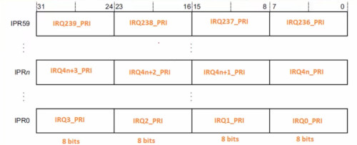
void GPIO_IRQPriorityConfig(uint8_t IRQNumber, uint8_t IRQPriority)
{
    // There are 60 PR Register and they are sets of 32-bits where each register is 8 bits
    uint8_t ipr_section = IRQNumber / 4;          // Find the section for the 60 PR registers
    uint8_t ipr_section_slot = IRQNumber % 4;     // Find the slot 4 x 8-bit registers

    // The amount of bits depends of the manufacturer
    // For ST the is 4
    uint8_t shift_amount = ( 8 * ipr_section_slot) + (8 - NO_PR_BITS_IMPLEMENTED);

    *(NVIC_PR_BASE_ADDR + ipr_section) |= (IRQPriority  << shift_amount );
}
Set Enable/Clear Register for IRQ (Processor Side)
To enable/disable the IRQ we need to enable the correct NVIC_ISER or NVIC_ICER. In the driver header we set these at the top. These addresses can be found in the Cortex m4.
// Interrupt Set-Enable Register
#define NVIC_ISER0        ( (volatile uint32_t*) 0xE000E100 )
#define NVIC_ISER1        ( (volatile uint32_t*) 0xE000E104 )
#define NVIC_ISER2        ( (volatile uint32_t*) 0xE000E108 )
#define NVIC_ISER3        ( (volatile uint32_t*) 0xE000E10C )

// Interrupt Clear-Enable Register
#define NVIC_ICER0        ( (volatile uint32_t*) 0xE000E180 )
#define NVIC_ICER1        ( (volatile uint32_t*) 0xE000E184 )
#define NVIC_ICER2        ( (volatile uint32_t*) 0xE000E188 )
#define NVIC_ICER3        ( (volatile uint32_t*) 0xE000E18C )
We can create a function in the GPIO driver to set and clear based on IRQ in the driver.
void GPIO_IRQInterruptConfig(uint8_t IRQNumber, uint8_t EnableOrDisable)
{
    // Not % used to find bit position give IRQ is 0-95
    // Position 34 is 34 / 32 gives remainder 2 i.e. position 2
    if (EnableOrDisable == ENABLE)
    {
        if (IRQNumber < 32)
        {
            *NVIC_ISER0 |= (uint32_t)(1 << IRQNumber);
        }
        else if (IRQNumber > 31 && IRQNumber < 64)
        {
            // Program ISER1
            *NVIC_ISER1 |= (1 << IRQNumber % 32);
        }
        else if (IRQNumber > 63 && IRQNumber < 96)
        {
            // Program ISER2
            *NVIC_ISER2 |= (1 << IRQNumber % 64);
        }
    }
    else
    {
        if(IRQNumber < 32) {
            // Program ICER0
            *NVIC_ICER0 |= (1 << IRQNumber);
        } else if(IRQNumber > 31 && IRQNumber < 64) {
            // Program ICER1
            *NVIC_ICER1 |= (1 << IRQNumber  % 32);
        } else if(IRQNumber > 63 && IRQNumber < 96) {
            // Program ICER2
            *NVIC_ICER2 |= (1 << IRQNumber % 64);
        }
    }
}
Clear EXTI PR Register for GPIO Pin (Peripheral Side)
When we want to implement an IRQ handler we need to clear the EXIT PR register by writing 1 for that GPIO pin
void GPIO_IRQHandling(uint8_t PinNumber)
{
    // If the Register is set to 1 for this bit
    //    We clear it  by writing 1
    //    This confused by but presumably this is event driven
    if(EXTI->PR & ( 1 << PinNumber)) {

        // Clear
        EXTI->PR |= (1 << PinNumber );

    }
}
Implement Override IRQ Handler (Application)
Implementing the handler is the easiest part. Default handlers are provided in the .s file provided with the board and run at startup. In the startup code in the .s you will see
.w EXTI0_IRQHandler
.tumb_set EXTI0_IRQHandler, Default_Handler
To override this we need to create a function of the same name in the main. The handler takes no arguments or returns any arguments. We pass the GPIO Pin number to our driver code from above.
// Overriden from .s file
void EXTI0_IRQHandler(void) {
    GPIO_IRQHandling(0);
}
SPI
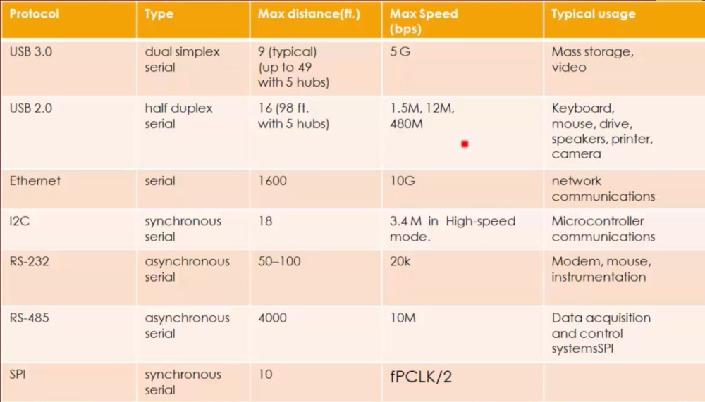
Next we are looking at SPI. Below is a list of possible protocols and usage for MCUs
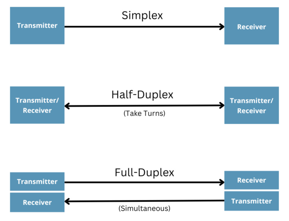
There are 3 SPI modes. These are shown below. Some SPI devices might not support all.
NSS Slave Select Management
On the slave we can manage the NSS pin for SPI using the SPIx_CR1 register for STM32. This allow us, when SSM=1, to ground the state via the SSI value, SSI=0 is grounded, SSI=1 is pulled high. This frees up the NSS pin for other usage. Otherwise we need to ground this pin.
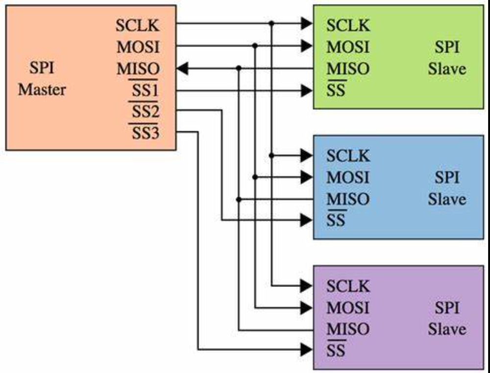
Where there are multiple slaves you would not use the NSS pin and this would be tied to vdd (high). Separate pins would be used instead for each slave so they can be used independantly.
Communication format
We need to be aware of
- SCLK Phase (CPHA)
- SCLK Polarity (CPOL)
- Data Frame Format (DFF)
Clearly we need both ends to be using the same approach. For the Data Frame Format this is 8-bit or 16-bit depending on MCU. Here is a view of the CLK Phase and Polarity if unconvinced they must be the same.
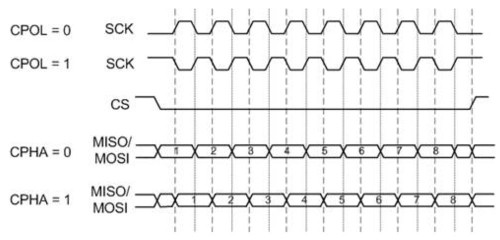
You will need to check the documentation of which mode CPHA/CPOL and device can be configured to.
Other Stuff
Memory Hierarchy
There is a Hierarchy
- Registers
- Cache (L1 Local, L2 Shared)
- Main Memory (RAM)
- Long Term Storage (Hard Disks, Tapes etc)
Types Of Memory
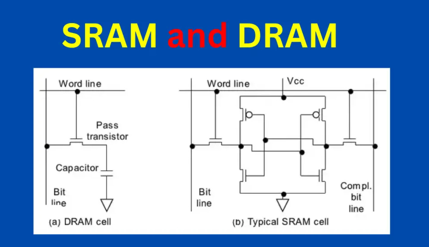
- DRAM Dynamic RAM uses capacitors, slower, cheaper, requires refreshing
- SRAM Static RAM uses transistors, faster
Types Of Addressing Memory
These are the types of addressing.
- Random Address (RAM)
- Direct Addressing (HDD)
- Sequential Addressing (Tapes)
- Associative Addressing (Caching)
Speed and Cost Per Bit change goes down as performance goes down.
Cache Memory
Introduction
Terms
- Miss Element was not found
- Hit Element was found
- Hit Rate Percentage of time that element was found
Effective Access Time =
   Hit Rate * Time from Cache  + (1 - Hit rate) - time from Memory
Looking at examples, it was the hit rate that the tutor wanted us to focus on as the other parts would not change.
For loops indicate to the compiler that we will probably access data more than once and maybe its neighbours.
Types of Associative Cache
There are 3 types of associative addressing cache algorithms
- Fully Associative
- Direct Mapping
- Set Associative
Each of the approaches uses tag value approach where the tag is part of the address and the value is organized to allow to find the element
Fully Associative
For this approach the Full address is split between the Block ID and a number of bits known as the Word ID. The Block ID becomes the Tag. And the value is divided into slots based on the size of the word ID.
- 1-bits 2 elements are stored slot-0, slot-1
- 2-bits 4 elements are stored slot-0, slot-1, slot-2,-slot-3
This is shown below

The values are replaced in the case using a replacement alogorthm such as
- FIFO First in First Out
- LRU Least Recently Used. Replaced Block least used
- LFU Least Frequently Used. Replaced Block least frequently used
- Random Just pick one
This approach has the least chance of thrashing but is expensive and slow.
Direct Mapping
For this approach we use the more of the address to store a line ID. The Full Address is not split into
- Tag first part of address
- Line ID, which line of the cache to store data in
- Word ID, as before the slot for the data in the value
This does not need a replacement algorithm and is therefore fast and cheap. But given the line IDs means data can be replaced often it is prone to thrashing.
Set Associative
This is similar to the above example where instead of a Line ID, a Set ID is stored. I.E. the cache has n rows size of set ID. Shown below is a line ID of 2-bits so each row has two slots. For this approach we do need a replacement algorithm. This approach is used by raspberry PI and many manufacturers

Flags in Cache
Along with tag and value there are flags associated with a row. They are
- Type Data or Instructrion
- Valid Whether valid
- Lock Lock flag
- Dirty bit - Identifies a line of data that has been written to but not been updated
Memory Device Interface
Here was shown how the circuit might work with D Flip-Flops and a clock line. Added was an address decoders to allow the device to select the right clock line. Three other signals are required, a write, a read and a chip select.

Ironically he went on to show this device which I reckon is the one I am using for the 6502.
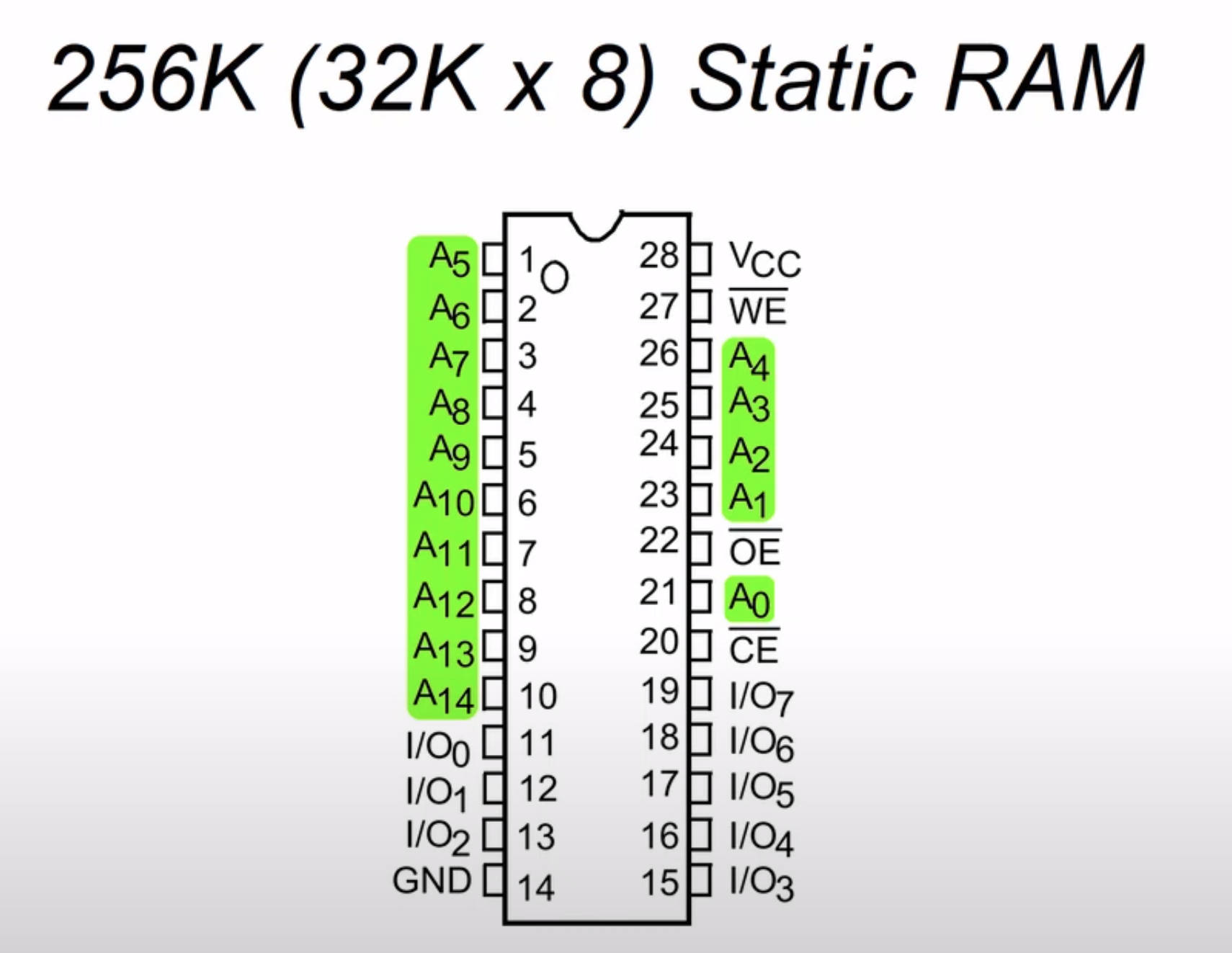
Chip Select
When we look at an MCU there is a memory map which shows where the peripherals are on the device. Each device has a range of memory used to operate it.
There are address lines within the mcu which are connected to the device. In the example below there are 20 address lines and the Graphic Card is located between 0xE0000 and 0xFFFFF. Putting this number into binary shows that address lines A19-A17 is the CS (Chip Select) and address line A16-A00 is the graphic card. Setting A19-A17 to binary 111 effectively means you are using the address lines for the graphics card.

In order to operate the correct memory device from the processor you use the correct chip select.
To maybe see a real world example here is windows showing us the memory map range for a device.

