Verilog
Introduction
Dipping my toe into this now I own an fpga
Boolean Algebra
Symbols (crash)
Hardest thing about this is the amount of different symbols which mean the same thing.
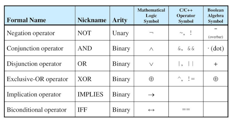
I guess each party wanted there own way. Here are the gates as seen on a circuit diagram
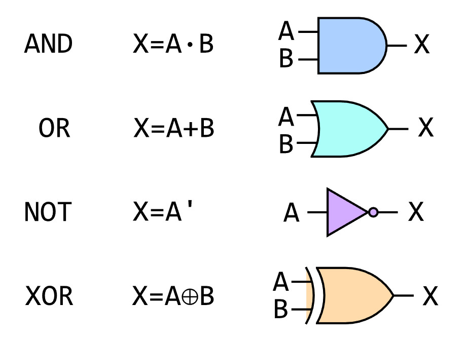
And of course someone else knew better. Here is IEEE version but given the amount of googling to get one nice enough I am guessing these are not popular

This seemed to be the popular way for documentr a truth table where NOT uses a macron over the value to indicate inverted (negated) value.
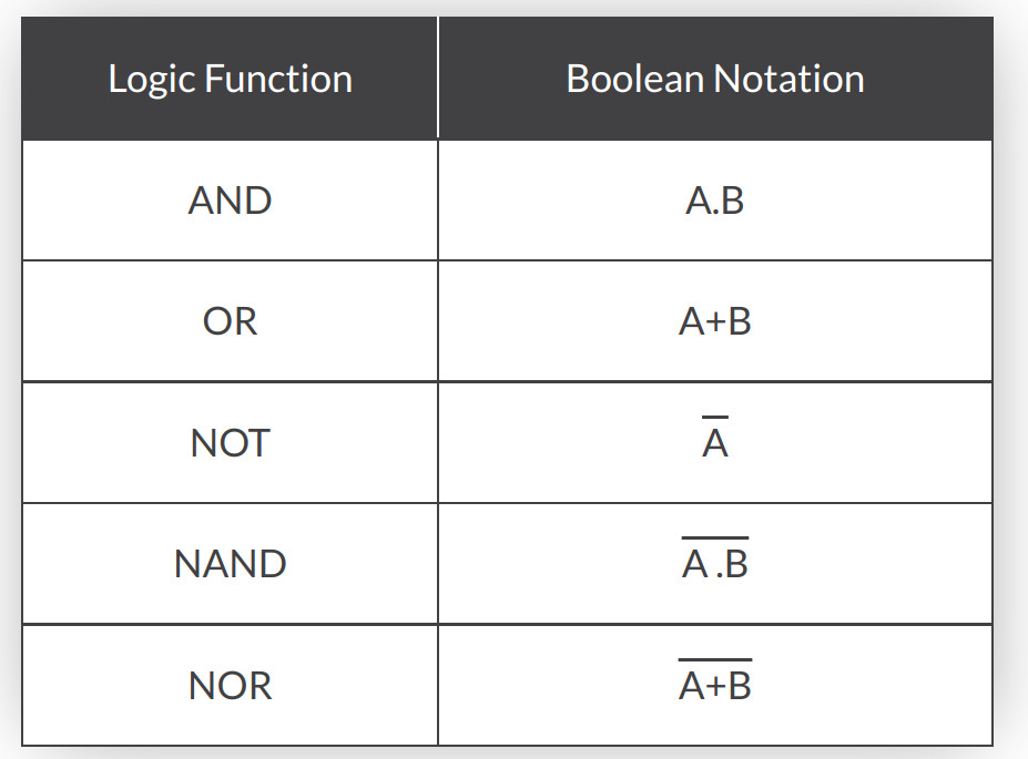
Work XOR example
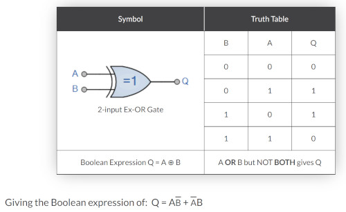
Really liked this explanation for XOR from youtube which combines all elements learning today. Truth tables are 2 to the power of inputs.
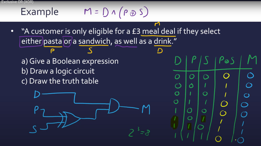
XOR Explanation
I write this not in order. But further down I struggled with the boolean algebra for XOR gates and the substitution. Below is the explanation for which it works. Here is the truth table
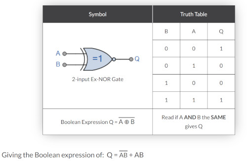
NOR Explanation
And here is the NOR gate equivalent. It really is not as hard as it looks once you are in the zone. Wright the truth table and the algebra and ezzy pezzy.
Boolean Laws
Commutative Law
Any binary operation which satisfies the following expression is referred to as a commutative operation. Commutative law states that changing the sequence of the variables does not have any effect on the output of a logic circuit.
- A. B = B. A
- A + B = B + A
Associative Law
It states that the order in which the logic operations are performed is irrelevant as their effect is the same.
- ( A. B ). C = A . ( B . C )
- ( A + B ) + C = A + ( B + C)
Distributive Law
Distributive law states the following conditions:
- A. ( B + C) = (A. B) + (A. C)
- A + (B. C) = (A + B) . ( A + C)
AND Law
These laws use the AND operation. Therefore they are called AND laws.
- A .0 = 0
- A . 1 = A
- A. A = A
OR Law
These laws use the OR operation. Therefore they are called OR laws.
- A + 0 = A
- A + 1 = 1
- A + A = A
Inversion Law
In Boolean algebra, the inversion law states that double inversion of variable results in the original variable itself.
Boolean Algebra Theorems
De Morgan’s First Law
De Morgan’s First Law states that the complement of the product of the variables is equal to the sum of their individual complements of a variable.
(A.B)’ = A’+B’
or
¬(A.B) = ¬A + ¬B
or
¬(A AND B) = ¬A OR ¬B
De Morgan’s Second Law
The second law states that the complement of the sum of variables is equal to the product of their individual complements of a variable.
(A+B)’ = A’.B’
or
¬(A+B) = ¬A . ¬B
or
¬(A OR B) = ¬A AND ¬B
Why Always me favourite Question
When we put logic on a circuit we can use these to help reduce the amount of components, therefore cost and errors.
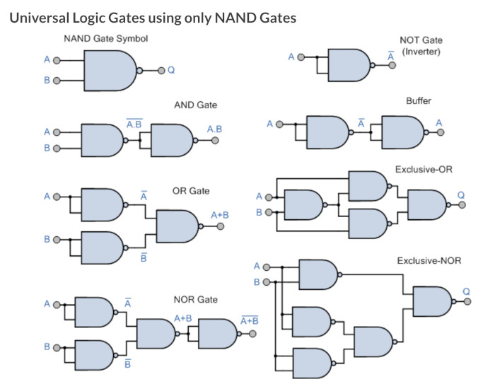
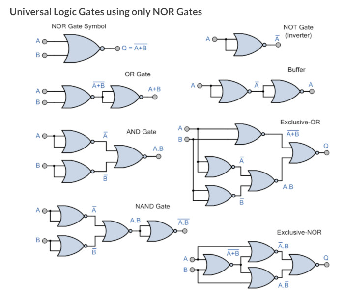
A little distraction Universal Gates
During the demonstration of using the De Morgon theorems, it was shown that you can make any gate from either NAND or NOR gates so thought I might put these here.
Back to Dave
Here is an example for Dave a eevblog (my hero today)
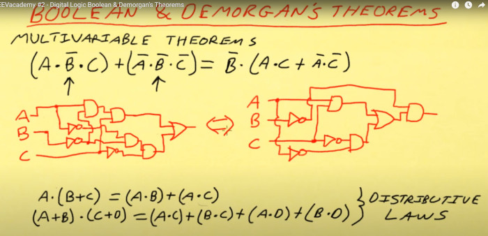
Using the above knowledge we have reduced the components from 5 input gates, 3 invertors, to 4 input gates, 3 invertors just using the distributive laws.
Below is Dave explaining an easy way to remember De Morgans's first theroem. Drop the bar and change the sign
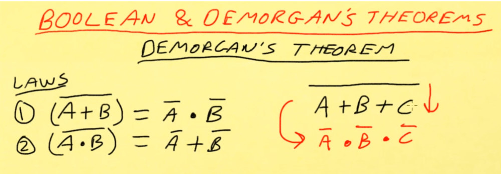
We can now start spotting patterns where we know we can reduce the gate count. Here we have two input NOR gates as inputs to a NOR gate. Using boolean algebra we can reduce this to an AND gate

Hello World
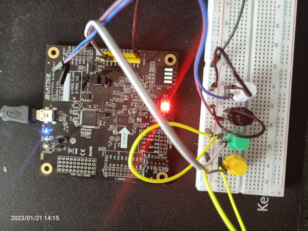
This is the first program. There are two files to get it to work, a pcf file which defines things you use in the verilog file. Currently my understanding is it maps hardware to names which you can reference in the verilog file. Here is the project. I only use two buttons in the example but there are four shown for the second example
 ==Requirements
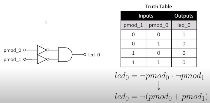
For the requirements we have only light when both buttons are pressed.
Truth Table
We can express this as a circuit diagram and a truth table. We need to understand some boolean algebra to understand the truth table
PCF Physical Constraints File (and_gate.pcf)
Could not find a lexer but here we define names to io pins. You lookup the pin in the datasheet, in my case a ice40UP5K-B-EVN and you assign a name.
#LED
set_io              led_0  41

#HEADER B I/O
set_io  -pullup yes pmod_0 23
set_io  -pullup yes pmod_1 25
Verilog File (and_gate.v)
Here is my first program, it defines two input buttons and 1 LED in a module called and_gate. The value of LED is true when pmod_0 and pmod_1 are true.
module and_gate (
    // inputs
    input   pmod_0,
    input   pmod_1,

    // Outputs
    output  led_0
);

    assign led_0 = ~pmod_0 & ~pmod_1;

endmodule
Hello World 2
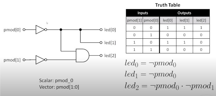
Well now we have the basics we can add some more verilog stuff. We can reference the inputs and outputs as arrays. We are now going to build a circuit where if we press 1 button, 2 LEDs light up and if we press 2 buttons 2 LED light up. This is shown in the circuit diagram and truth table below
PCF Physical Constraints File (and_gate.pcf)
Not we can put the hardware in array to make the verilog file simpler
#LED
set_io    led[0]  23
set_io    led[1]  25
set_io    led[2]  26
#set_io    led[3]  27
#set_io    led[4]  32

set_io  -pullup yes pmod[0] 36
set_io  -pullup yes pmod[1] 42

#set_io  -pullup yes pmod_2 12
#set_io  -pullup yes pmod_3 14
Verilog File (and_gate.v)
Here is my first program. We basically create a name for the wiring not_pod_0 and assign LED 0,1 to one value and LED 2 to another.
module and_gate (
    // inputs
    input   [1:0] pmod,

    // Outputs
    output  [2:0] led
);

    // Wire declaration
    wire not_pod_0;

    // Continuous Assignment replicate 1 wire to two outputs
    assign not_pmod_0 = ~pmod[0];
    assign led[1:0] = {2{not_pmod_0}};

    // Continuous Assignment: NOT and AND operators
    assign led[2] = not_pmod_0 & ~pmod[1];

endmodule
True Adder
Truth Table
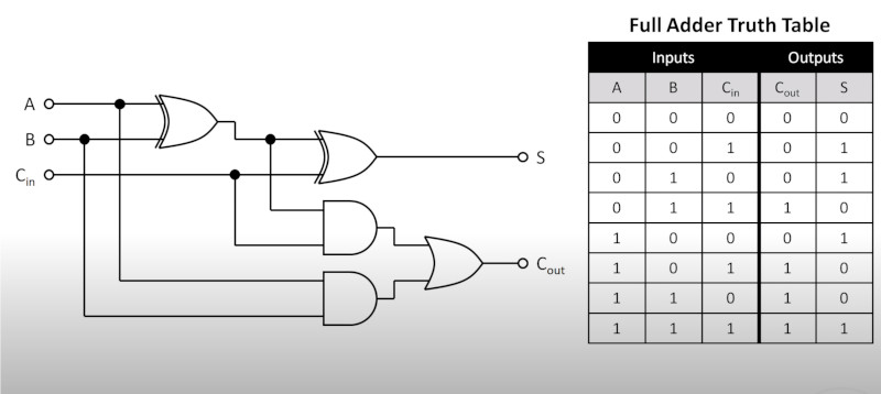
Next we make a truth adder using the following
The Cᵢₙ represents the carry value. So you add A + B and the carry to get column S. If there is a carry then Cₒᵤₜ is 1
Boolean Algebra representation
Doing my own attempt and it took a couple because it is hard to see the bars and we have
S    = (A̅.B̅.C ) +  (A̅.B.C̅) + (A.B̅.C̅) + (A.B.C)
Cₒᵤₜ = (A̅.B.C ) +  (A.B̅.C) + (A.B.C̅) + (A.B.C̅)
Now we need to simplify
Simplification of S
Here is the Simplification of S
Lets take C as common and pair up with 1st and 4th expression and 2 and 3

=> C ( A̅.B̅ + A.B )  + C̅ (A̅.B + A.B̅)

Found this a bit tricky to wrote up the XOR and NOR above. Basically A̅.B̅ + A.B = A̅ ⊕ B̅ - XOR and A̅.B + A.B̅ = A ⊕ B - NOR
=> C ( A̅ ⊕ B̅ ) + C̅ ( A ⊕ B)

Lets substitute A̅ ⊕ B̅ = x this gives
=> Cx̅ + C̅x Compliments result in XOR
=> C ⊕ x

 Substituting x back in
=> C ⊕ A ⊕ B
Simplification of Cₒᵤₜ
Here is the Simplification of Cₒᵤₜ
 Lets take C as common for 1 and 2 and AB to 3 and 4
=> C ( A̅B + AB̅) + AB (C + C̅)

 Using OR law (Z + Z̅ = 1) we can apply this to the Right hand side
=> C ( A̅B + AB̅) + AB
Using compliments
=> C (A̅ ⊕ B̅) + AB
PCF File
Perhaps the only part I found simple
#LEDS
set_io    led[0]  23
set_io    led[1]  25
set_io    led[2]  26
set_io    led[3]  27
set_io    led[4]  32

#Push Buttons
set_io  -pullup yes pmod[0] 36
set_io  -pullup yes pmod[1] 42
set_io  -pullup yes pmod[2] 38
set_io  -pullup yes pmod[3] 28
Verilog File
Not that hard but do need to understand there result. Here is mine
module full_adder (

    // Inputs
    input   [2:0]   pmod,

    // Output
    output  [1:0]   led
);
    wire A;
    wire B;
    wire C;

    // Set A, B, and C  to buttons and off
    assign A = ~pmod[0];
    assign B = ~pmod[1];
    assign C = ~pmod[2];

    // Taken from above working
    // led[0] C (A̅ ⊕ B̅) + AB
    // led[1] C ⊕ A ⊕ B

    // Cout
    assign led[0] = (C & (!A ^ !B) ) | (A & B);

    // S
    assign led[1] = C ^ A ^ B;


endmodule