Verilog
Introduction
Dipping my toe into this now I own an fpga
Hello World
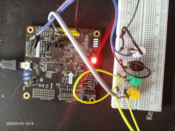
This is the first program. There are two files to get it to work, a pcf file which defines things you use in the verilog file. Currently my understanding is it maps hardware to names which you can reference in the verilog file. Here is the project. I only use two buttons in the example but there are four shown for the second example
 ==Requirements
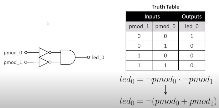
For the requirements we have only light when both buttons are pressed.
Truth Table
We can express this as a circuit diagram and a truth table. We need to understand some boolean algebra to understand the truth table
PCF Physical Constraints File (and_gate.pcf)
Could not find a lexer but here we define names to io pins. You lookup the pin in the datasheet, in my case a ice40UP5K-B-EVN and you assign a name.
#LED
set_io              led_0  41

#HEADER B I/O
set_io  -pullup yes pmod_0 23
set_io  -pullup yes pmod_1 25
Verilog File (and_gate.v)
Here is my first program, it defines two input buttons and 1 LED in a module called and_gate. The value of LED is true when pmod_0 and pmod_1 are true.
module and_gate (
    // inputs
    input   pmod_0,
    input   pmod_1,

    // Outputs
    output  led_0
);

    assign led_0 = ~pmod_0 & ~pmod_1;

endmodule
Hello World 2
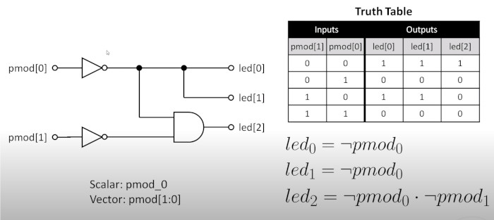
Well now we have the basics we can add some more verilog stuff. We can reference the inputs and outputs as arrays. We are now going to build a circuit where if we press 1 button, 2 LEDs light up and if we press 2 buttons 2 LED light up. This is shown in the circuit diagram and truth table below
PCF Physical Constraints File (and_gate.pcf)
Not we can put the hardware in array to make the verilog file simpler
#LED
set_io    led[0]  23
set_io    led[1]  25
set_io    led[2]  26
#set_io    led[3]  27
#set_io    led[4]  32

set_io  -pullup yes pmod[0] 36
set_io  -pullup yes pmod[1] 42

#set_io  -pullup yes pmod_2 12
#set_io  -pullup yes pmod_3 14
Verilog File (and_gate.v)
Here is my first program. We basically create a name for the wiring not_pod_0 and assign LED 0,1 to one value and LED 2 to another.
module and_gate (
    // inputs
    input   [1:0] pmod,

    // Outputs
    output  [2:0] led
);

    // Wire declaration
    wire not_pod_0;

    // Continuous Assignment replicate 1 wire to two outputs
    assign not_pmod_0 = ~pmod[0];
    assign led[1:0] = {2{not_pmod_0}};

    // Continuous Assignment: NOT and AND operators
    assign led[2] = not_pmod_0 & ~pmod[1];

endmodule
Inverting of Buttons
As I get more familar with this I realize that the assign can be used to control the fact that buttons work in reverse. We use a pullup resister to ensure the button is on by default. We can reverse this be using assign
module full_adder (
    // Inputs
    input   pmod,
);
    wire A;
    assign A = ~pmod;
...
True Adder
Truth Table
Next we make a truth adder using the following
The Cᵢₙ represents the carry value. So you add A + B and the carry to get column S. If there is a carry then Cₒᵤₜ is 1
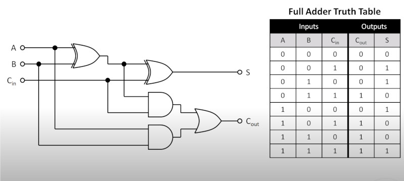
Boolean Algebra representation
Doing my own attempt and it took a couple because it is hard to see the bars and we have
S    = (A̅.B̅.C ) +  (A̅.B.C̅) + (A.B̅.C̅) + (A.B.C)
Cₒᵤₜ = (A̅.B.C ) +  (A.B̅.C) + (A.B.C̅) + (A.B.C̅)
Now we need to simplify
Simplification of S
Here is the Simplification of S
Lets take C as common and pair up with 1st and 4th expression and 2 and 3

=> C ( A̅.B̅ + A.B )  + C̅ (A̅.B + A.B̅)

Found this a bit tricky to wrote up the XOR and NOR above. Basically A̅.B̅ + A.B = A̅ ⊕ B̅ - XOR and A̅.B + A.B̅ = A ⊕ B - NOR
=> C ( A̅ ⊕ B̅ ) + C̅ ( A ⊕ B)

Lets substitute A̅ ⊕ B̅ = x this gives
=> Cx̅ + C̅x Compliments result in XOR
=> C ⊕ x

 Substituting x back in
=> C ⊕ A ⊕ B
Simplification of Cₒᵤₜ
Here is the Simplification of Cₒᵤₜ
 Lets take C as common for 1 and 2 and AB to 3 and 4
=> C ( A̅B + AB̅) + AB (C + C̅)

 Using OR law (Z + Z̅ = 1) we can apply this to the Right hand side
=> C ( A̅B + AB̅) + AB
Using compliments
=> C (A̅ ⊕ B̅) + AB
PCF File
Perhaps the only part I found simple
#LEDS
set_io    led[0]  23
set_io    led[1]  25
set_io    led[2]  26
set_io    led[3]  27
set_io    led[4]  32

#Push Buttons
set_io  -pullup yes pmod[0] 36
set_io  -pullup yes pmod[1] 42
set_io  -pullup yes pmod[2] 38
set_io  -pullup yes pmod[3] 28
Verilog File
Not that hard but do need to understand there result. Here is mine
module full_adder (

    // Inputs
    input   [2:0]   pmod,

    // Output
    output  [1:0]   led
);
    wire A;
    wire B;
    wire C;

    // Set A, B, and C  to buttons and off
    assign A = ~pmod[0];
    assign B = ~pmod[1];
    assign C = ~pmod[2];

    // Taken from above working
    // led[0] C (A̅ ⊕ B̅) + AB
    // led[1] C ⊕ A ⊕ B

    // Cout
    assign led[0] = (C & (!A ^ !B) ) | (A & B);

    // S
    assign led[1] = C ^ A ^ B;


endmodule
Digi-Keys Solution
Learning Verilog using the digi-key [tutorial]. Mine works but as is my want I need to understand the differences
- leds are reversed
- led[0] and my solution are identical we just need to define a_xor_b
- led[1] I need to understand how ( (a ^ b) & c_in) in their solution = (C & (!A ^ !B) ) in my solution
So here is my explanation for why (A ^ B) = (!A ^ !B)
 We know A ^ B =  A!B + !AB because of the XOR above
 If we substitute A and B with there negatives
 We get A!B + !AB which is A^B
module full_adder (

    // Inputs
    input   [2:0]   pmod,

    // Output
    output  [1:0]   led
);

    // Wire (net) declarations (internal to module)
    wire a;
    wire b;
    wire c_in;
    wire a_xor_b;

    // A, B, and C_IN are inverted button logic
    assign a = ~pmod[0];
    assign b = ~pmod[1];
    assign c_in = ~pmod[2];

    // Create intermediate wire (net)
    assign a_xor_b = a ^ b;

    // Create output logic
    assign led[0] = a_xor_b ^ c_in;
    assign led[1] = (a_xor_b & c_in) | (a & b);
endmodule
Always and Registers
The next example is to demonstrate how these work. Hopefully comments in line make it obvious
module button_counter (

    // Inputs
    input   [2:0]   pmod,

    // Output
    output  reg [3:0]   led
);

    wire rst;
    wire clk;

    assign rst = ~pmod[0];
    assign clk = ~pmod[1];

    // Like a loop
    // while(clk or rst) {
    //   if(rst){
    //     led[0-3] = b0
    //   } else {
    //     led[ led[current] +1] = b1
    //   }
    // }

    always @(posedge clk or posedge rst) begin
        if(rst == 1'b1) begin
            led <= 4'b0;
        end else begin
            led <= led + 1'b1;
        end
    end
endmodule
Clocks
Got this to work and understood it. Cannot seem to replace clock with crystal clearly more to learn.
module button_counter (

    // Inputs
    input               clk,
    input               rst_btn,

    // Output
    output  reg [3:0]   led
);
    wire rst;

    // Create some registers
    reg div_clk;
    reg [31:0] count;

    // 10110111000110110000000 = 6000000 in Binary

    localparam [31:0] max_count = 6000000;

    // Reset is the inverse of the reset button
    assign rst = ~rst_btn;

    // Count up on (divided) clock rising edge or reset on button push
    // while (div_clk or reset) {
    //    if (reset == 1) {
    //       led[0-3] = 0
    //    }
    //    else {
    //       led[ led[current] +1] = b1
    //    }
    // }
    always @ (posedge div_clk or posedge rst) begin
        if (rst == 1'b1) begin
            led <= 4'b0;
        end else begin
            led <= led + 1'b1;
        end
    end

    // Count up on (divided) clock rising edge or reset on button push
    // while (clk or reset) {
    //    if (reset == 1) {
    //       count[0-31] = 0
    //    }
    //    else if (count = max_count) {
    //       count[0-31] = 0
    //       div_clk = !div_clk;
    //    }
    //    else {
    //       count = count +1
    //    }
    // }
    always @ (posedge clk or posedge rst) begin
        if (rst == 1'b1) begin
            count <= 32'b0;
        end else if (count == max_count) begin
            count <= 32'b0;
            // Revisiting this, it was this line I struggled with but the answer is pretty easy
            // One invert the value if the max_count has been achieved. We invert because we don't know if it is one or zero
            div_clk <= ~div_clk;
        end else begin
            count <= count + 1;
        end
    end

endmodule
Mealy and Moore Finite State Machines (FSM)
Finite State Machines
Thought I knew about these. Turns out I need to match knowledge to theory. Here is how we show finite state machines. Either with a table or a diagram. The circles represent states and the double circles are what is called accepeting states.
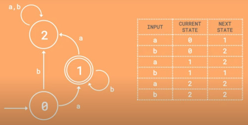
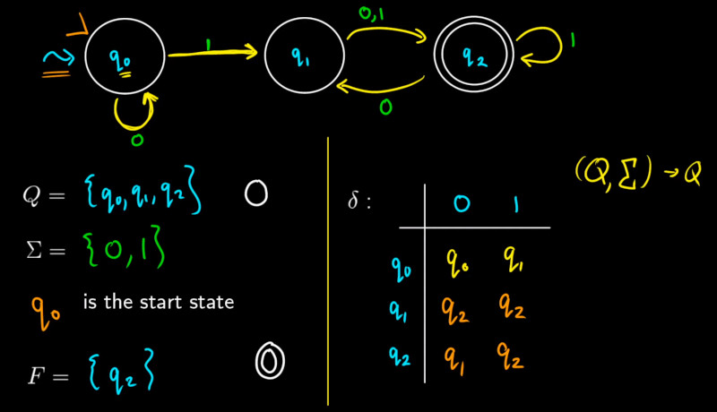
Working through the logic we find it is just fancy language which is good because we can communicate and understand each other.
- Q is a finite set of states.
- ∑ is a finite set of symbols called the alphabet.
- 8δ is the transition function where δ: Q × ∑ → Q
- q0 is the initial state from where any input is processed (q0 ∈ Q).
- F is a set of final state/states of Q (F ⊆ Q).
Looking at the video kinda explained it all. Note there is a arrow usually to show the start state.
Verilog State Machine Examples
Moore and Mearly State Machine
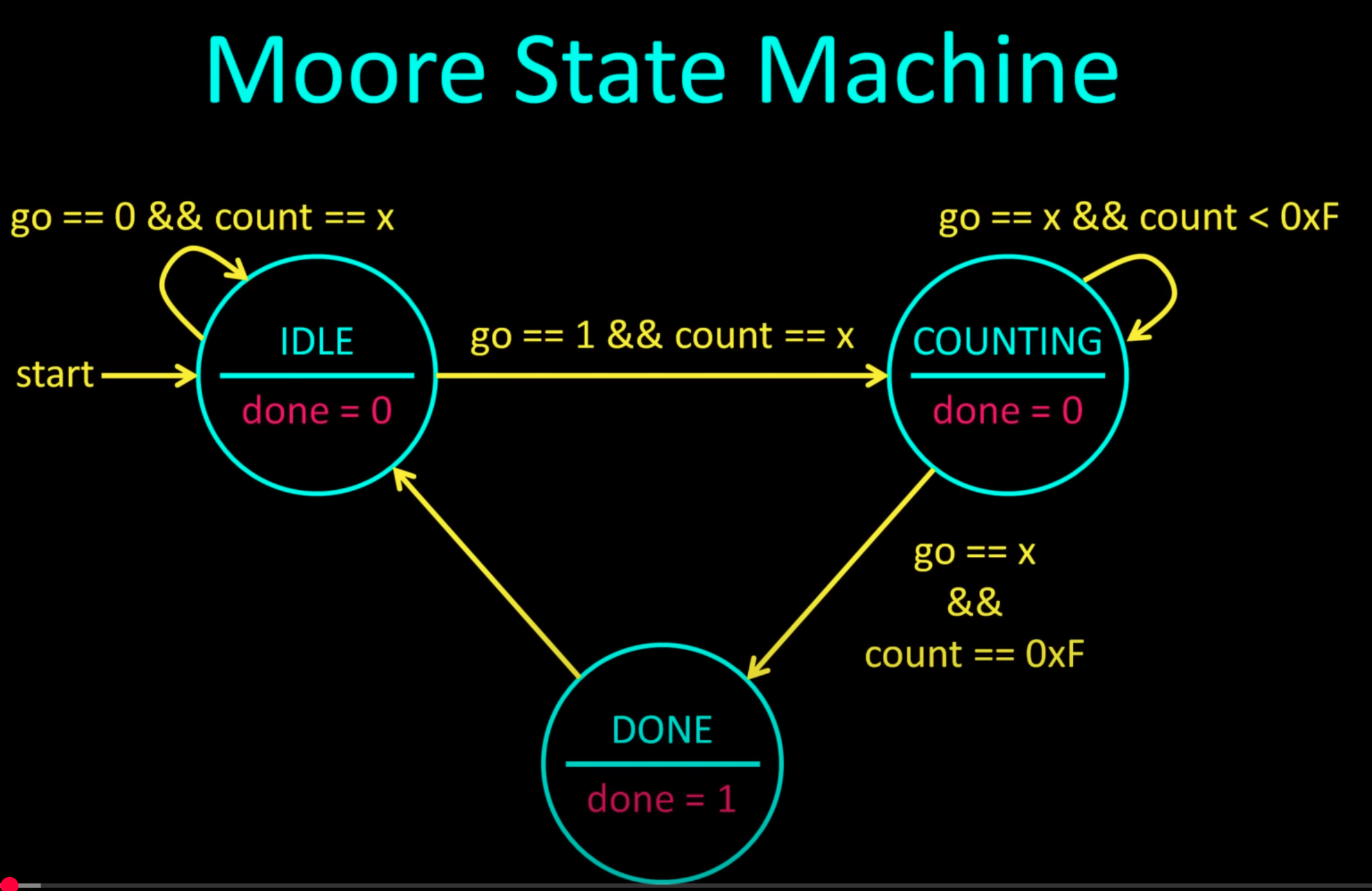
In the example we were shown both moore and mealy state machines for the same requirements
Moore
Mealy
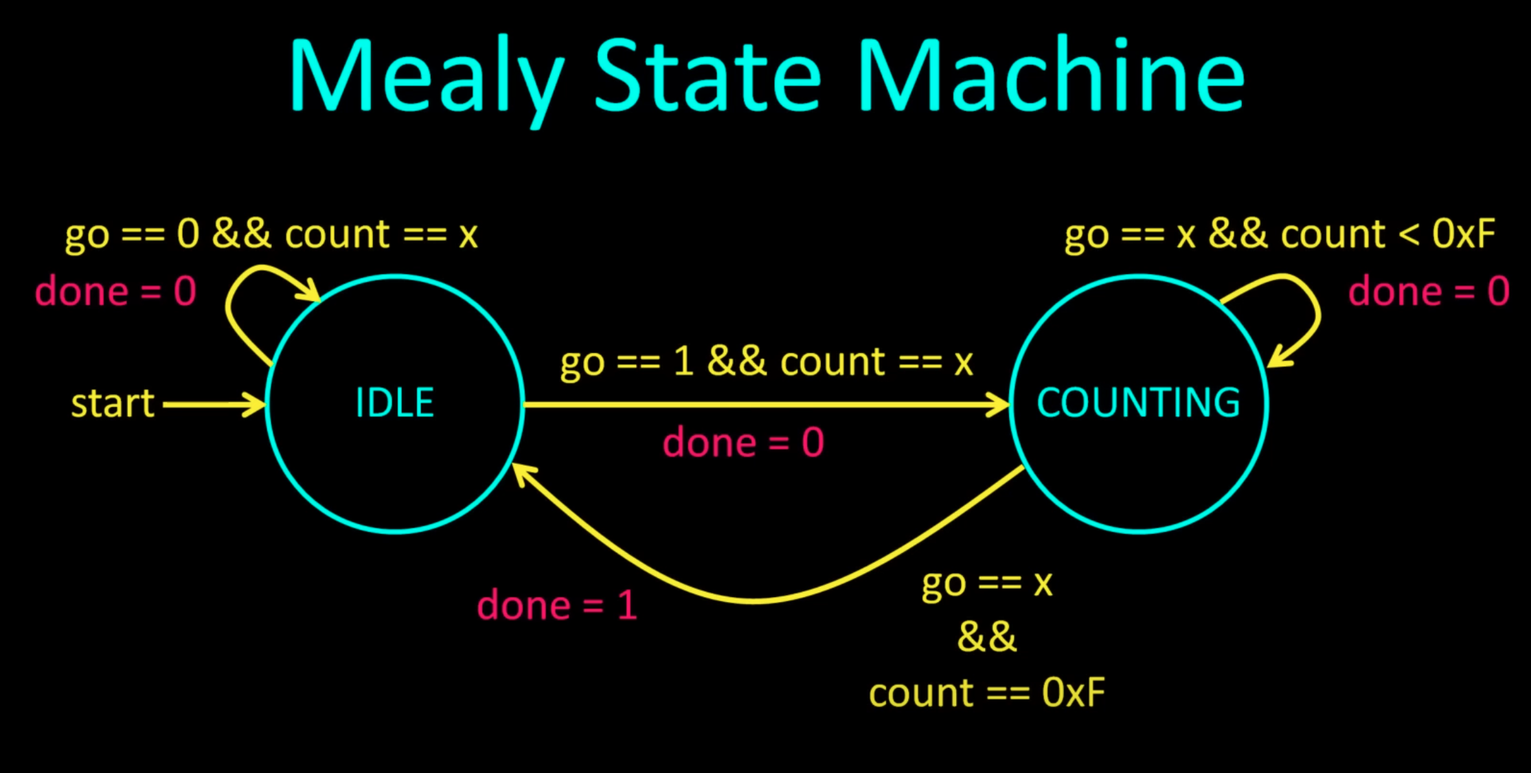
A chapter that actually made sense. It was suggested the moore state machine was easier to read but moore states to handle.
Moore State Machine
module moore_fsm (

    // Inputs
    input               clk,
    input               rst_btn,
    input               go_btn,

    // Outputs
    output  reg [3:0]   led,
    output  reg         done_sig
);

    // States
    localparam  STATE_IDLE      = 2'd0;
    localparam  STATE_COUNTING  = 2'd1;
    localparam  STATE_DONE      = 2'd2;

    // Max counts for clock divider and counter
    localparam  MAX_CLK_COUNT   = 24'd1500000;
    localparam  MAX_LED_COUNT   = 4'hF;

    // Internal signals
    wire rst;
    wire go;

    // Internal storage elements
    reg         div_clk;
    reg [1:0]   state;
    reg [23:0]  clk_count;

    // Invert active-low buttons
    assign rst = ~rst_btn;
    assign go = ~go_btn;

    // Clock divider
    always @ (posedge clk or posedge rst) begin
        if (rst == 1'b1) begin
            clk_count <= 24'b0;
        end else if (clk_count == MAX_CLK_COUNT) begin
            clk_count <= 24'b0;
            div_clk <= ~div_clk;
        end else begin
            clk_count <= clk_count + 1;
        end
    end

    // State transition logic
    always @ (posedge div_clk or posedge rst) begin

        // On reset, return to idle state
        if (rst == 1'b1) begin
            state <= STATE_IDLE;

        // Define the state transitions
        end else begin
            case (state)

                // Wait for go button to be pressed
                STATE_IDLE: begin
                    if (go == 1'b1) begin
                        state <= STATE_COUNTING;
                    end
                end

                // Go from counting to done if counting reaches max
                STATE_COUNTING: begin
                    if (led == MAX_LED_COUNT) begin
                        state <= STATE_DONE;
                    end
                end

                // Spend one clock cycle in done state
                STATE_DONE: state <= STATE_IDLE;

                // Go to idle if in unknown state
                default: state <= STATE_IDLE;
            endcase
        end
    end

    // Handle the LED counter
    always @ (posedge div_clk or posedge rst) begin
        if (rst == 1'b1) begin
            led <= 4'd0;
        end else begin
            if (state == STATE_COUNTING) begin
                led <= led + 1;
            end else begin
                led <= 4'd0;
            end
        end
    end

    // Handle done LED output
    always @ ( * ) begin
        if (state == STATE_DONE) begin
            done_sig = 1'b1;
        end else begin
            done_sig = 1'b0;
        end
    end

endmodule
Mearly State Machine
module mealy_fsm (

    // Inputs
    input               clk,
    input               rst_btn,
    input               go_btn,

    // Outputs
    output  reg [3:0]   led,
    output  reg         done_sig
);

    // States
    localparam STATE_IDLE       = 2'd0;
    localparam STATE_COUNTING   = 2'd1;
    localparam STATE_DONE       = 2'd2;

    // Not the letter before the value is the type
    // b = binary
    // d = decimal
    // h = hex
    // Max counts for clock divider and counter
    localparam MAX_CLK_COUNT    = 24'd1500000;
    localparam MAX_LED_COUNT    = 4'hf;

    // Internal signals
    wire rst;
    wire go;

    // Internal storage elements
    reg         div_clk;
    reg [1:0]   state;
    reg [23:0]  clk_count;

    // Invert active-low buttons
    assign rst = ~rst_btn;
    assign go = ~go_btn;

    // clock divider no change except for values
    always @ (posedge clk or posedge rst) begin
        if (rst == 1'b1) begin
            clk_count <= 24'b0;
        end else if (clk_count == MAX_CLK_COUNT) begin
            clk_count <= 24'b0;
            div_clk <= ~div_clk;
        end else begin
            clk_count <= clk_count + 1;
        end
    end


    // State transition logic
    always @ (posedge div_clk or posedge rst) begin

        // On reset, return to idle state and restart counters
        if (rst == 1'b1) begin
            state <= STATE_IDLE;

        // Define the state transitions
        end else begin
            case (state)

                // Wait for go button to be pressed
                STATE_IDLE: begin
                    if (go == 1'b1) begin
                        state <= STATE_COUNTING;
                    end
                end

                // Go from counting to done if counting reaches max
                STATE_COUNTING: begin
                    if (led == MAX_LED_COUNT) begin
                        state <= STATE_DONE;
                    end
                end

                // Default case: return to idle state
                default: state <= STATE_IDLE;
            endcase
        end
    end

    // Run counter if in wait state
    always @ (posedge div_clk or posedge rst) begin
        if (rst == 1'b1) begin
            led <= 4'd0;
        end else begin
            if (state == STATE_COUNTING) begin
                led <= led + 1;
            end else begin
                led <= 4'd0;
            end
        end
    end

    always @ ( * ) begin
        if (state == STATE_DONE) begin
            done_sig = 1'b1;
        end else begin
            done_sig = 1'b0;
        end
    end

endmodule
Verilog Modules 2024
Pretty pretty please to be doing new stuff. Been a journey for me. Anyway on with the show. This is the FPGA part 6 from digikey and introduces modules which are what they sound like. It show me the glue between modules had changes which will make this a tad longer than expected. First the module which is the clock divider we did before except we now use parameter for the values we want to be able to set differently.
Passing Parameters
There two ways to do this the old way and the new way. For modules you seem to be able to mix and match.
Old Way
module clock_divider (

    // Inputs
    input       clk,
    input       rst,

    // Outputs
    output  reg out
);

    // Parameters
    parameter                   COUNT_WIDTH = 24;
    parameter [COUNT_WIDTH:0]   MAX_COUNT   = 6000000 - 1;

    // Internal signals
    wire rst;
    reg div_clk;
    reg [COUNT_WIDTH:0] count;

    // Clock divider
    always @ (posedge clk or posedge rst) begin
        if (rst == 1'b1) begin
            count <= 0;
            out <= 0;
        end else if (count == MAX_COUNT) begin
            count <= 0;
            out <= ~out;
        end else begin
            count <= count + 1;
        end
    end
endmodule
And now here is an example of using the module
module main (

    // Inputs
    input           clk,
    input           rst_btn,

    // Outputs
    output  [1:0]   led         // Not reg element!
);

    // Internal signals
    wire rst;

    // Invert active-low button
    assign rst = ~rst_btn;

    // Instantiate the first clock divider module
    clock_divider div_1 (
        .clk(clk),
        .rst(rst),
        .out(led[0])
    );
    defparam div_1.COUNT_WIDTH  = 32;
    defparam div_1.MAX_COUNT    = 1500000 - 1;

    // Instantiate the second clock divider module
    clock_divider div_2 (
        .clk(clk),
        .rst(rst),
        .out(led[1])
    );
endmodule
Ansi Way
module main (

    // Inputs
    input           clk,
    input           rst_btn,

    // Outputs
    output  [1:0]   led         // Not reg element!
);

    // Internal signals
    wire rst;

    // Invert active-low button
    assign rst = ~rst_btn;

    // Instantiate the first clock divider module
    clock_divider #(.COUNT_WIDTH(32), .MAX_COUNT(1500000 - 1)) div_1 (
        .clk(clk),
        .rst(rst),
        .out(led[0])
    );

    // Instantiate the second clock divider module
    clock_divider div_2 (
        .clk(clk),
        .rst(rst),
        .out(led[1])
    );

endmodule
And now here is an example of using the module
module clock_divider #(
    parameter                   COUNT_WIDTH = 24,
    parameter [COUNT_WIDTH:0]   MAX_COUNT   = 6000000 - 1
) (

    // Inputs
    input       clk,
    input       rst,

    // Outputs
    output  reg out
);

    // Internal signals
    // wire rst;
    reg div_clk;
    reg [COUNT_WIDTH:0] count;

    // Clock divider
    always @ (posedge clk or posedge rst) begin
        if (rst == 1'b1) begin
            count <= 0;
            out <= 0;
        end else if (count == MAX_COUNT) begin
            count <= 0;
            out <= ~out;
        end else begin
            count <= count + 1;
        end
    end

endmodule
Using the Test Bed
This was a bit full-on, maybe me. There is alot to unpick. In the video they test the clock divider module above. This links in nicely with my work on pulseview. Getting the duration an scale right it important.
The initial keyword means what is says and I guess the is pretty obvious what it does. The dumpvars first parameter determines the depth the measures are for. E.g. 0 is everything. I think 1 means just the clock_divider module.
// Defines timescale for simulation: <time_unit> / <time_precision>
`timescale 1 ns / 10 ps

// Define our testbench
module clock_divider_tb();

    // Internal signals
    wire    out;

    // Storage elements (set initial values to 0)
    reg     clk = 0;
    reg     rst = 0;

    // Simulation time: 10000 * 1 ns = 10 us
    localparam DURATION = 10000;

    // Generate clock signal: 1 / ((2 * 41.67) * 1 ns) = 11,999,040.08 MHz
    always begin

        // Delay for 41.67 time units
        // 10 ps precision means that 41.667 is rounded to 41.67
        #41.667

        // Toggle clock line
        clk = ~clk;
    end

    // Instantiate the unit under test (UUT)
    clock_divider #(.COUNT_WIDTH(4), .MAX_COUNT(6 - 1)) uut (
        .clk(clk),
        .rst(rst),
        .out(out)
    );

    // Pulse reset line high at the beginning
    initial begin
        #10
        rst = 1'b1;
        #1
        rst = 1'b0;
    end

    // Run simulation (output to .vcd file)
    initial begin

        // Create simulation output file
        $dumpfile("clk-div_tb.vcd");
        $dumpvars(0, clock_divider_tb);

        // Wait for given amount of time for simulation to complete
        #(DURATION)

        // Notify and end simulation
        $display("Finished!");
        $finish;
    end

endmodule
Memory
Overview
More concepts. Really enjoying some of my other knowledge joining up. In the video they mentioned the types of memory an fpga.
- Distributed RAM - This is when the data is store in the Lookup tables (LUTs)
- EBR (Embedded block RAM) - These are configurable memory chunks. You can set the width, depth and other characteristics
- SPRAM (Single Port Synchronous RAM) - Larger than block RAM
On my fpga ice40up5k-b-evn we have
- 4 x 256k SPRAM
- 120 kbits (120000 bits) EBR
We have the following configurations for EB RAM
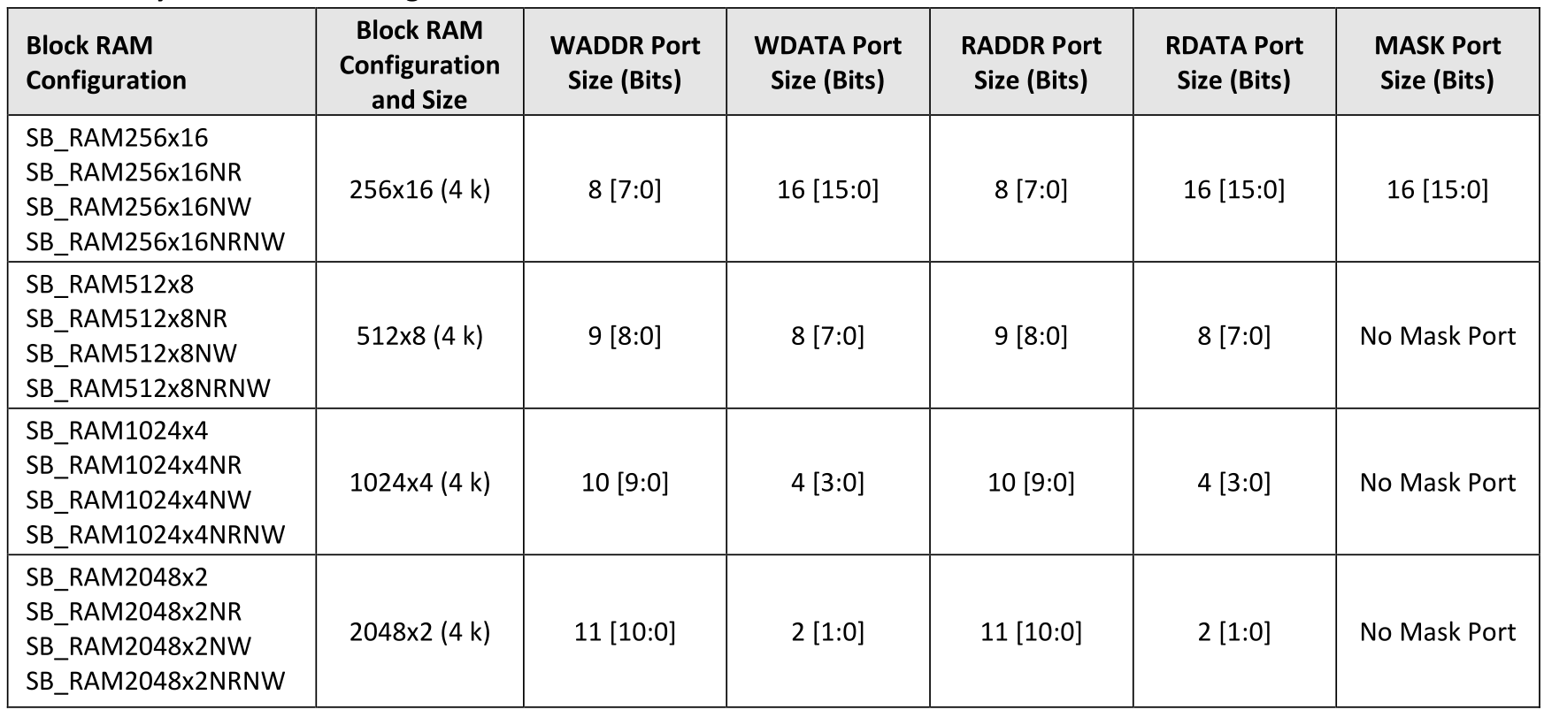
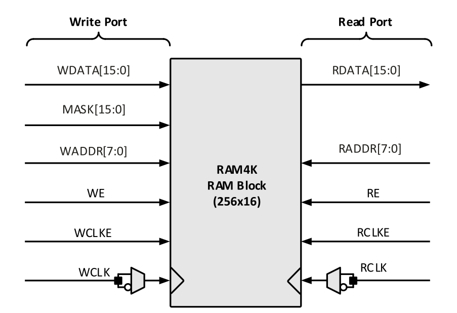
Signals for the EB RAM
Signals for the SPRAM

Once you use a block of RAM you cannot use another part of the block for something else.
Memory Module
Here is a basic memory module. The inputs, outputs are as expected and we read and write when the enabled is set.
// Inferred block RAM
module memory #(

    // Parameters
    parameter   INIT_FILE = ""
) (

    // Inputs
    input               clk,
    input               w_en,
    input               r_en,
    input       [3:0]   w_addr,
    input       [3:0]   r_addr,
    input       [7:0]   w_data,

    // Outputs
    output  reg [7:0]   r_data
);

    // Declare memory
    reg [7:0]  mem [0:15];

    // Interact with the memory block
    always @ (posedge clk) begin

        // Write to memory
        if (w_en == 1'b1) begin
            mem[w_addr] <= w_data;
        end

        // Read from memory
        if (r_en == 1'b1) begin
            r_data <= mem[r_addr];
        end
    end

    // Initialization (if available)
    initial if (INIT_FILE) begin
        $readmemh(INIT_FILE, mem);
    end

endmodule
Testing Again
So this shows a test bed where we read in from a file to drive the test.
`timescale 1 ns / 10 ps

// Define our testbench
module memory_tb();

    // Internal signals
    wire    [7:0]  r_data;


    // Storage elements (set initial values to 0)
    reg             clk = 0;
    reg             w_en = 0;
    reg             r_en = 0;
    reg     [3:0]   w_addr;
    reg     [3:0]   r_addr;
    reg     [7:0]   w_data;
    integer         i;

    // Simulation time: 10000 * 1 ns = 10 us
    localparam DURATION = 10000;

    // Generate clock signal: 1 / ((2 * 41.67) * 1 ns) = 11,999,040.08 MHz
    always begin
        #41.67
        clk = ~clk;
    end

    // Instantiate the unit under test (UUT)
    memory #(.INIT_FILE("mem_init.txt")) uut (
        .clk(clk),
        .w_en(w_en),
        .r_en(r_en),
        .w_addr(w_addr),
        .r_addr(r_addr),
        .w_data(w_data),
        .r_data(r_data)
    );

    // Run test: write to location and read value back
    initial begin

        // Test 1: read initial values
        for (i = 0; i < 16; i = i + 1) begin
            #(2 * 41.67)
            r_addr = i;
            r_en = 1;
            #(2 * 41.67)
            r_addr = 0;
            r_en = 0;
        end

        // Test 2: Write to address 0x0f and read it back
        #(2 * 41.67)
        w_addr = 'h0f;
        w_data = 'hA5;
        w_en = 1;
        #(2 * 41.67)
        w_addr = 0;
        w_data = 0;
        w_en = 0;
        r_addr = 'h0f;
        r_en = 1;
        #(2 * 41.67)
        r_addr = 0;
        r_en = 0;

        // Test 3: Read and write at same time
        #(2 * 41.67)
        w_addr = 'h0a;
        w_data = 'hef;
        w_en = 1;
        r_addr = 'h0a;
        r_en = 1;
        #(2 * 41.67)
        w_addr = 0;
        w_data = 0;
        w_en = 0;
        r_addr = 0;
        r_en = 0;
    end

    // Run simulation (output to .vcd file)
    initial begin

        // Create simulation output file
        $dumpfile("memory_tb.vcd");
        $dumpvars(0, memory_tb);

        // Wait for given amount of time for simulation to complete
        #(DURATION)

        // Notify and end simulation
        $display("Finished!");
        $finish;
    end

endmodule
Device Utilization
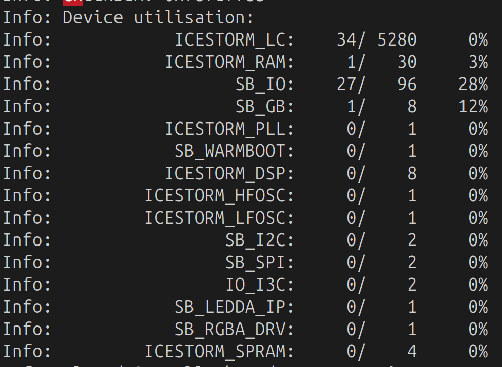
Before doing the test they built the software with apio build -v and then showed that
apio build -v
Because of this you needed real pins in the PCF otherwise the build would fail. The point of this was to look at the output of the build and realize the usage. Useful when designing
Another Reminder
- Clock cycles are the time for a clock to rise and fall. | ̄|_|
icestick
- there is a 12 Mhz Clock on a icestick
- Generate 12 Million Cycles per second
- Given 1 Microsecond is 1 millionth of a second this means there are 12 cycles per microsecond
- A clock divider of 6000000 will mean we are a 1 Mhz as there is a rising and falling edge
- We need 24bits to store 6000000
We can demonstrate the with gtkwave. Assuming we have faked our clock-divider correctly we can see the out is now only 1 clock cycle per 12 clock cycles or the actual clock. Therefore the out line is now 1 Mhz

In the icestick test bed we create a delay of 41.67 to simulate the clock using the following formula
1 / ((2 * 41.67) * 1 ns) = 11,999,040.08 MHz
ice40UP5K
Reading the docs it looked like the ice40UP5K had a 48Mhz clock so I wrote this. But it is the same as the icestick 12Mhz
- there is a 48 Mhz Clock on a ice40UP5K
- Generate 48 Million Cycles per second
- Given 1 Microsecond is 1 millionth of a second this means there are 48 cycles per microsecond
- A clock divider of 24000000 will mean we are a 1 Mhz as there is a rising and falling edge
- We need 26bits to store 6000000
We can demonstrate the with gtkwave. Assuming we have faked our clock-divider correctly we can see the out is now only 1 clock cycle per 48 clock cycles or the actual clock. Therefore the out line is now 1 Mhz

In the ice40UP5K test bed we create a delay of 41.67 to simulate the clock using the following formula
1 / ((2 * 10.417) * 1 ) = 47,998,464.0491 MHz
Gotcha
Cost a bit of time to understand my error with this. When we write the test bed we scale the date back and don't do a second. I got confused with reality and testing. We scale back the values to reduce the output
Big Project (for me)
This is a big project. We are going to
- collect a button sequence
- store it in memory
- play it back
Star of the Show - Not
So this look like a easy task and indeed I have now learned a lot about debugging. Setting lights on so you know it is working. The problem was caused by
$readmemh(INIT_FILE, mem);
In the video that provide the code and it looked like this
0
0
0
0
1
1
1
1
This was to populate the following verilog
    // Declare memory
    // Width = 2, Depth = 8
    reg [MEM_WIDTH - 1:0]  mem [0:MEM_DEPTH - 1];
Reading the documents it looks like you need to use the following format to make it work.
03
00
01
00
02
00
01
00
But this did mean I learned more about verilog figuring it out.
Clock Divider
This is the same as above with parameters for count width and max_count.
Memory
This is the same as before but we pass the depth and the width of the memory we are using. This did introduce System Verilog and the use of the function $clog2. I think that the system verilog can be transpiled to verilog. Anyway here it is.
module memory #(

    // Parameters
    parameter   MEM_WIDTH = 16,
    parameter   MEM_DEPTH = 256,
    parameter   INIT_FILE = ""
) (

    // Inputs
    input               clk,
    input               w_en,
    input               r_en,
    input       [ADDR_WIDTH - 1:0]   w_addr,
    input       [ADDR_WIDTH - 1:0]   r_addr,
    input       [MEM_WIDTH - 1:0]  w_data,

    // Outputs
    output  reg [MEM_WIDTH - 1:0]  r_data
);

    // Calculate the number of bits required for the address
    localparam  ADDR_WIDTH = $clog2(MEM_DEPTH);

    // Declare memory
    reg [MEM_WIDTH - 1:0]  mem [0:MEM_DEPTH - 1];

    // Interact with the memory block
    always @ (posedge clk) begin

        // Write to memory
        if (w_en) begin
            mem[w_addr] <= w_data;
        end

        // Read from memory
        if (r_en) begin
            r_data <= mem[r_addr];
        end
    end

    // Initialization (if available)
    initial if (INIT_FILE) begin
        $readmemh(INIT_FILE, mem);
    end

endmodule
Debouncing
This is when you press once but it registers a few times. We don't want this and to avoid it we create a module with a state machine to control it.
module debouncer #(

    // Max counts for wait state (40 ms with 12 MHz clock)
    parameter                   COUNT_WIDTH     = 20,
    parameter [COUNT_WIDTH:0]   MAX_CLK_COUNT   = 480000 - 1
) (

    // Inputs
    input               clk,
    input               rst,
    input               in,

    // Outputs
    output  reg         out
);

    // States
    localparam  STATE_HIGH      = 2'd0;
    localparam  STATE_LOW       = 2'd1;
    localparam  STATE_WAIT      = 2'd2;
    localparam  STATE_PRESSED   = 2'd3;

    // Internal storage elements
    reg [1:0]           state;
    reg [COUNT_WIDTH:0] clk_count;

    // State transition logic
    always @ (posedge clk or posedge rst) begin

        // On reset, return to idle state
        if (rst == 1'b1) begin
            state <= STATE_HIGH;
            out <= 1'b0;

        // Define the state transitions
        end else begin
            case (state)

                // Wait for increment signal to go from high to low
                STATE_HIGH: begin
                    out <= 1'b0;
                    if (in == 1'b0) begin
                        state <= STATE_LOW;
                    end
                end

                // Wait for increment signal to go from low to high
                STATE_LOW: begin
                    if (in == 1'b1) begin
                        state <= STATE_WAIT;
                    end
                end

                // Wait for count to be done and sample button again
                STATE_WAIT: begin
                    if (clk_count == MAX_CLK_COUNT) begin
                        if (in == 1'b1) begin
                            state <= STATE_PRESSED;
                        end else begin
                            state <= STATE_HIGH;
                        end
                    end
                end

                // If button is still pressed
                STATE_PRESSED: begin
                    out <= 1'b1;
                    state <= STATE_HIGH;
                end

                // Default case: return to idle state
                default: state <= STATE_HIGH;
            endcase
        end
    end

    // Run counter if in wait state
    always @ (posedge clk or posedge rst) begin
        if (rst == 1'b1) begin
            clk_count <= 0;
        end else begin
            if (state == STATE_WAIT) begin
                clk_count <= clk_count + 1;
            end else begin
                clk_count <= 0;
            end
        end
    end

endmodule
Top Module
module sequencer_top #(

    // Parameters
    parameter   DEBOUNCE_COUNTS = 480000 - 1,   // Counts for debounce wait
    parameter   STEP_COUNTS = 6000000 - 1,      // Clock cycles between steps
    parameter   NUM_STEPS = 8                   // Number of steps

) (

    // Inputs
    input               clk,
    input               rst_btn,
    input               set_btn,
    input               ptn_0_btn,
    input               ptn_1_btn,

    // Outputs
    output  reg [1:0]   led,
    output              test_led,
    output      [1:0]   unused_led
);

    // Internal signals
    wire            rst;
    wire            set;
    wire            set_d;
    wire    [1:0]   ptn;
    wire            div_clk;
    wire    [1:0]   r_data;

    // Storage elements (initialize some values)
    reg             w_en = 0;
    reg             r_en = 1'b1;    // Always high!
    reg     [2:0]   w_addr = 0;
    reg     [2:0]   r_addr;
    reg     [1:0]   w_data;
    reg     [2:0]   step_counter;
    reg     [2:0]   mem_ptr = 0;

    // Turn off unused LEDs
    assign unused_led = 2'b00;

    // Invert active-low buttons
    assign rst = ~rst_btn;
    assign set = ~set_btn;
    assign ptn[0] = ~ptn_0_btn;
    assign ptn[1] = ~ptn_1_btn;

    // Clock divider
    clock_divider #(
        .COUNT_WIDTH(24),
        .MAX_COUNT(STEP_COUNTS)
    ) div (
        .clk(clk),
        .rst(rst),
        .out(div_clk)
    );

    // Button debouncer for set buttons
    debouncer #(
        .COUNT_WIDTH(24),
        .MAX_CLK_COUNT(DEBOUNCE_COUNTS)
    ) set_debouncer (
        .clk(clk),
        .rst(rst),
        .in(set),
        .out(set_d)
    );

    // Memory unit
    memory #(
        .MEM_WIDTH(2),
        .MEM_DEPTH(NUM_STEPS),
        .INIT_FILE("mem_init.txt")
    ) mem (
        .clk(clk),
        .w_en(w_en),
        .r_en(r_en),
        .w_addr(w_addr),
        .r_addr(r_addr),
        .w_data(w_data),
        .r_data(r_data)
    );

    // Read from memory each divided clock cycle
    always @ (posedge div_clk or posedge rst) begin
        if (rst == 1'b1) begin
            led <= 0;
            r_addr <= 0;
            step_counter <= 0;
        end else begin
            r_addr <= step_counter;
            step_counter <= step_counter + 1;
            led <= r_data;
        end
    end

    // Register write data as soon as debounced set signal goes high
    always @ (posedge set_d) begin
        w_data <= ptn;
    end

    // Handle writing pattern to memory
    always @ (posedge clk or posedge rst) begin

        // Reset memory address pointer and write enable signal
        if (rst == 1'b1) begin
            mem_ptr <= 0;
            w_en <= 1'b0;

        // Set write enable high and increment memory pointer
        end else if (set_d == 1'b1) begin
            w_addr <= mem_ptr;
            w_en <= 1'b1;
            mem_ptr <= mem_ptr + 1;

        // Reset write enable signal
        end else begin
            w_en <= 1'b0;
        end
    end

endmodule
PLL (Phase Lock Loop)
This is a lot more theory than I would like but hey need to start somewhere. I guess the main question is whats it for and what is a PLL.
What a PLL for
If we use a divider to increase to voltage
What is a PLL
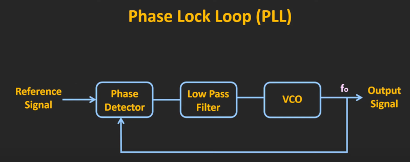
Pretty easy. Now we have to answer what is
- Phase Detector/Comparator
- Low Pass Filter
- VCO (Voltage Control Oscillator
Phase Detector/Comparator
This looks at the input and passes it on to the Low pass filter. For example if the voltage was too low from the VCO it would produce a positive error voltage. The output of the phase detector is in Volts/Radion.
2*π = 360degres
Low Pass Filter
VCO
This is easy to understand. You put in a voltage and it outputs some frequency. You raise the voltage and the frequency increases and vice versa
An Example
Well this was interesting. The example in the video gave the following code where the reference clock was pin 21 on the icestick. So I put in
module pll_test (

    // Inputs
    input               ref_clk,

    // Outputs
    output              clk
);

    // Instantiate PLL (120 MHz)
    SB_PLL40_CORE #(
        .FEEDBACK_PATH("SIMPLE"),   // Don't use fine delay adjust
        .PLLOUT_SELECT("GENCLK"),   // No phase shift on output
        .DIVR(4'b0000),             // Reference clock divider
        .DIVF(7'b1001111),          // Feedback clock divider
        .DIVQ(3'b011),              // VCO clock divider
        .FILTER_RANGE(3'b001)       // Filter range
    ) pll (
        .REFERENCECLK(ref_clk),     // Input clock
        .PLLOUTCORE(clk),           // Output clock
        .LOCK(),                    // Locked signal
        .RESETB(1'b1),              // Active low reset
        .BYPASS(1'b0)               // No bypass, use PLL signal as output
    );

endmodule
But this gave the following error

Obviously being an expert now in fpga meant I instantly recognize what was wrong. Anyway after hours of digging I found a site which helped. It told me I could not use pin 35 as a reference clock and had a few examples. I then start to understand a bit more about how this all fits together. The solution, shown below, show you can call a built in module to get a reference clock. The name seemed familar as it was the name from the reference manual. Here is the final solution from [damdoy]
module pll (
    // Outputs
    output              clk
);
   wire clk_48mhz; //internal

   //internal oscillators seen as modules
   SB_HFOSC SB_HFOSC_inst(
      .CLKHFEN(1),
      .CLKHFPU(1),
      .CLKHF(clk_48mhz)
   );

   SB_PLL40_CORE #(
      .FEEDBACK_PATH("SIMPLE"),
      .PLLOUT_SELECT("GENCLK"),
      .DIVR(4'b0000),
      .DIVF(7'b0010011),
      .DIVQ(3'b011),
      .FILTER_RANGE(3'b100)
    ) pll (
      .REFERENCECLK(clk_48mhz),
      .PLLOUTCORE(clk),
      .LOCK(),                    // Locked signal
      .RESETB(1'b1),
      .BYPASS(1'b0)
   );

endmodule
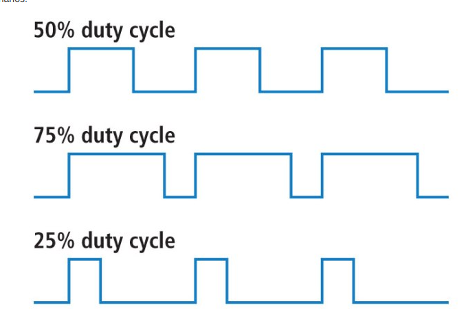
Duty Cycle
Probably mentioned this somewhere before but here goes again. Maybe a picture does say a thousand words. Pretty easy to understand. And when you attach an LED at 25% guess what happens to the brightness
